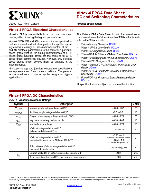
Description
Internal supply voltage relative to GND Auxiliary supply voltage relative to GND Output drivers supply voltage relative to GND Key memory battery backup supply Input reference voltage I/O input voltage relative to GND (all user and dedicated I/Os) I/O input voltage relative to GND (restricted to maximum of 100 user I/Os) (3,4) 2.5V or below I/O input voltage relative to GND (user and dedicated I/Os) –0.5 to 1.32 –0.5 to 3.0 –0.5 to 3.75 –0.5 to 4.05 –0.3 to 3.75 –0.75 to 4.05 –0.95 to 4.4 Units V V V V V V VIN (mercial Temperature) –0.85 to 4.3 (Industrial Temperature) V –0.75 to VCCO +0.5 ±100 ±200 V mA mA IIN Current applied to an I/O pin, powered or unpowered Total current applied to all I/O pins, powered or unpowered © 2004–2008 Xilinx, Inc. XILINX, the Xilinx logo, the Brand Window, and other designated brands included herein are trademarks of Xilinx, Inc.