XC5210
XC5210 is Field Programmable Gate Arrays manufactured by Xilinx.
- Part of the XC5200 comparator family.
- Part of the XC5200 comparator family.
Features
- Low-cost, register/latch rich, SRAM based reprogrammable architecture
- 0.5µm three-layer metal CMOS process technology
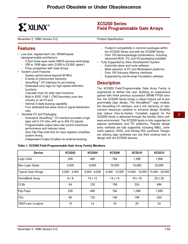
- 256 to 1936 logic cells (3,000 to 23,000 “gates”)
- Price petitive with Gate Arrays
- System Level Features
- System performance beyond 50 MHz
- 6 levels of interconnect hierarchy
- Versa Ring™ I/O Interface for pin-locking
- Dedicated carry logic for high-speed arithmetic functions
- Cascade chain for wide input functions
- Built-in IEEE 1149.1 JTAG boundary scan test circuitry on all I/O pins
- Internal 3-state bussing capability
- Four dedicated low-skew clock or signal distribution nets
- Versatile I/O and Packaging
- Innovative Versa Ring™ I/O interface provides a high logic cell to I/O ratio, with up to 244 I/O signals
- Programmable output slew-rate control maximizes performance and...