Datasheet4U Logo Datasheet4U.com

XC7V585T - Virtex-7 T and XT FPGAs

General Description

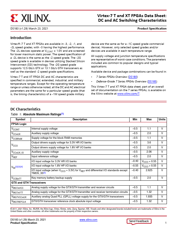
FPGA Logic VCCINT VCCAUX VCCBRAM VCCO Internal supply voltage Auxiliary supply voltage Supply voltage for the block RAM memories Output drivers supply voltage for 3.3V HR I/O banks Output drivers supply voltage for 1.8V HP I/O banks VCCAUX_IO VREF Auxiliary supply voltage Input reference voltag

📥 Download Datasheet

Full PDF Text Transcription for XC7V585T (Reference)

Note: Below is a high-fidelity text extraction (approx. 800 characters) for XC7V585T. For precise diagrams, and layout, please refer to the original PDF.

DS183 (v1.29) March 23, 2021 Virtex‐7 T and XT FPGAs Data Sheet: DC and AC Switching Characteristics Product Specification Introduction Virtex®-7 T and XT FPGAs are avail...

View more extracted text
Product Specification Introduction Virtex®-7 T and XT FPGAs are available in -3, -2, -1, and -2L speed grades, with -3 having the highest performance. The -2L devices operate at VCCINT = 1.0V and are screened for lower maximum static power. The speed specification of a -2L device is the same as the -2 speed grade. The -2G speed grade is available in devices utilizing Stacked Silicon Interconnect (SSI) technology. The -2G speed grade supports 12.5 Gb/s GTX or 13.1 Gb/s GTH transceivers as well as the standard -2 speed grade specifications. Virtex-7 T and XT FPGA DC and AC characteristics are specified in commercial, extend