XC7VX330T
Overview
(DS180)
- Defense-Grade 7 Series FPGAs Overview
(DS185) This Virtex-7 T and XT FPGA data sheet, part of an overall set of documentation on the 7 series FPGAs, is available on the Xilinx website at .xilinx./7.
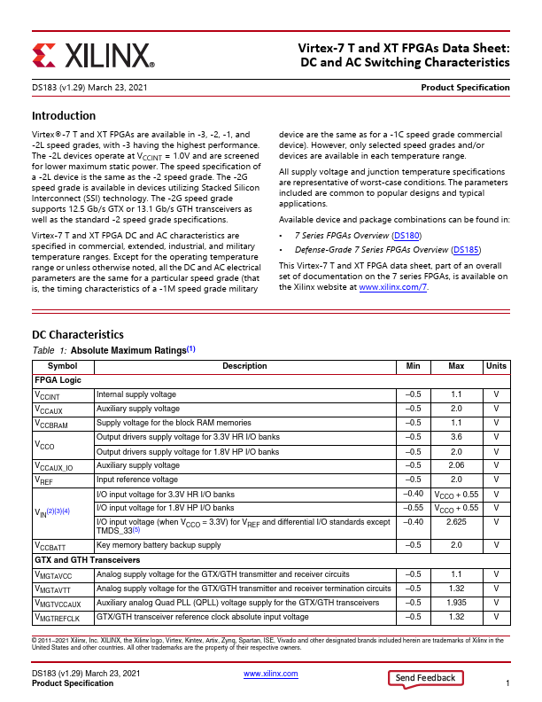
DC Characteristics
Table 1: Absolute Maximum Ratings(1)
Symbol
Description
FPGA Logic
VCCINT VCCAUX VCCBRAM
VCCO
Internal supply voltage Auxiliary supply voltage Supply voltage for the block RAM memories Output drivers supply voltage for 3.3V HR I/O banks Output drivers supply voltage for 1.8V HP I/O banks
VCCAUX_IO VREF
Auxiliary supply voltage Input reference voltage I/O input voltage for 3.3V HR I/O banks
VIN(2)(3)(4)
I/O input voltage for 1.8V HP I/O banks I/O input voltage (when VCCO = 3.3V) for VREF and differential I/O standards except TMDS_33(5)
VCCBATT
Key memory battery backup supply
GTX and GTH Transceivers
VMGTAVCC VMGTAVTT VMGTVCCAUX VMGTREFCLK
Analog supply voltage for the GTX/GTH transmitter and receiver circuits Analog supply voltage for...