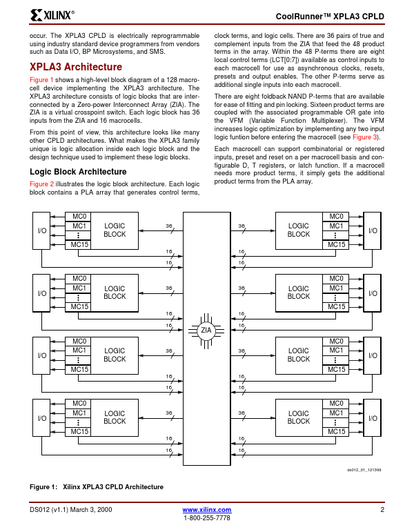
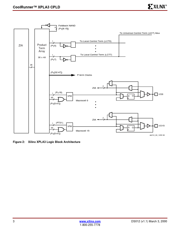
Xilinx XPLA3
the XPLA3 family includes Fast Zero Power (FZP) design technology that combines low power and high speed. With this design technique, the XPLA3 family offers true pin-to-pin speeds of 5.0 ns, while simultaneously delivering power that is less than 100 µA at standby without the need for "turbo bits" or other power down schemes. By replacing conventional sense amplifier methods for implementing product terms (a technique that has been used in PLDs since the bipolar era) with a cascaded chain of pure CMOS gates, the dynamic power is also substantially lower than any competing CPLD.| Part No. | XPLA3 |
|---|---|
| Datasheet | XPLA3 Download |
| Manufacturer |  Xilinx |
| Description | CPLD |
| Buy | Stock & Price |
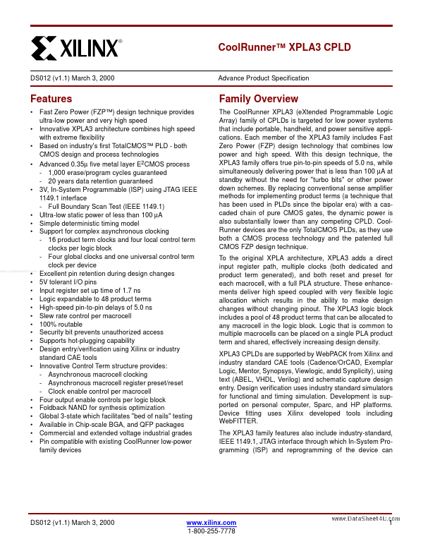
FEATURES
●●
●
● Fast Zero Power (FZP™) design technique provides ultra-low power and very high speed Innovative XPLA3 architecture combines high speed with extreme flexibility Based on industry's first TotalCMOS™ PLD - both CMOS design and process technologies Advanced 0.35µ five metal layer E2CMOS process - 1,000 erase/program cycles guaranteed - 20 years data retention guaranteed 3V, In-System Programmable (ISP) using JTAG IEEE 1149.1 interface - Full Boundary Scan Test (IEEE 1149.1) Ultra-low static power of less than 100 µA Simple deterministic timing model Support for complex asynchronous clocking - 16 product term clocks and four local control term clocks per logic block - Four global clocks and one universal control term clock per device Excellent pin retention during design changes 5V tolerant I/O pins Input register set up time of 1.7 ns Logic expandable to 48 product terms High-speed pin-to-pin delays of 5.0 ns Slew rate control per macrocell 100% routable Security bit preve...