XP5322GM
Description
XP5322 series are innovated design and silicon process technology to achieve the lowest possible on-resistance and fast switching performance. It provides the designer with an
G1 extreme efficient device for use in a wide range of power applications.
BVDSS RDS(ON) ID
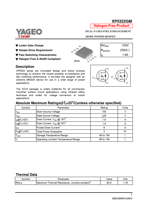
D1
G2 S1
100V 250mΩ
1.9A
D2
S2
The SO-8 package is widely preferred for all mercialindustrial surface mount applications using infrared reflow technique and suited for voltage conversion or switch applications.
Absolute Maximum Ratings@Tj=25o C(unless otherwise specified)
Symbol
Parameter
Rating
Units
Drain-Source Voltage
VGS ID@TA=25℃ ID@TA=70℃ IDM PD@TA=25℃ TSTG TJ
Gate-Source Voltage Drain Current, VGS @ 10V3 Drain Current, VGS @ 10V3 Pulsed Drain Current1
Total Power Dissipation
Storage Temperature Range
Operating Junction Temperature Range
+20
-55 to 150
℃
-55 to 150
℃
Thermal Data
Symbol Rthj-a
Parameter Maximum Thermal Resistance,...