XP9926GM
Description
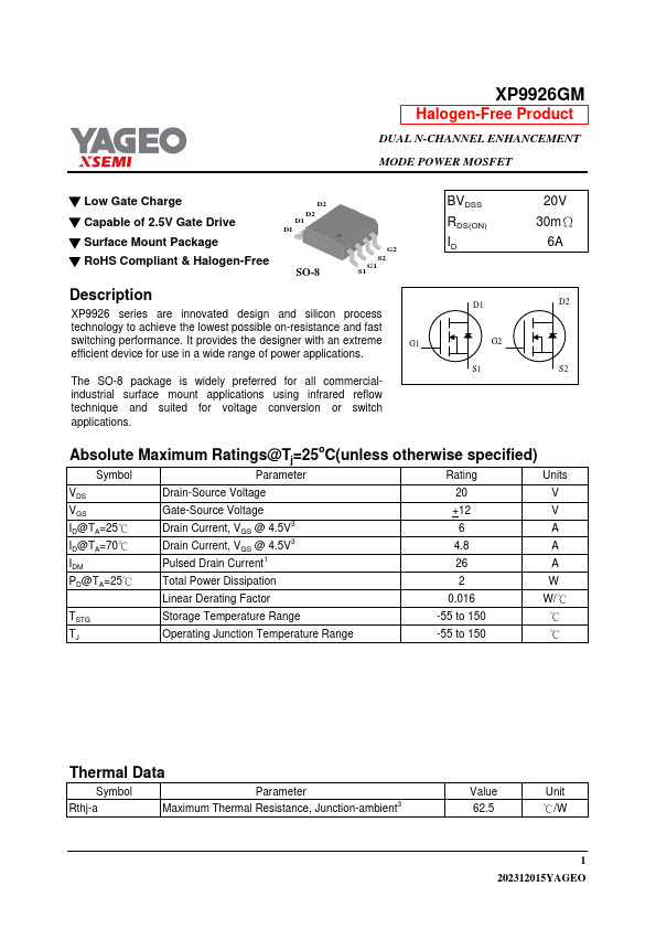
XP9926 series are innovated design and silicon process technology to achieve the lowest possible on-resistance and fast switching performance. It provides the designer with an extreme G1 efficient device for use in a wide range of power applications.
The SO-8 package is widely preferred for all mercialindustrial surface mount applications using infrared reflow technique and suited for voltage conversion or switch applications.
BVDSS RDS(ON) ID
D1
G2 S1
20V 30mΩ
6A
D2
S2
Absolute Maximum Ratings@Tj=25o C(unless otherwise specified)
Symbol
Parameter
Rating
Units
VDS VGS ID@TA=25℃ ID@TA=70℃ IDM PD@TA=25℃
Drain-Source Voltage
Gate-Source Voltage Drain Current, VGS @ 4.5V3 Drain Current, VGS @ 4.5V3 Pulsed Drain Current1
Total Power Dissipation
Linear Derating Factor
20 +12
6 4.8 26 2 0.016
V V A A A W W/℃
TSTG TJ
Storage Temperature Range Operating Junction Temperature Range
-55 to 150
℃
-55 to 150
℃
Thermal Data
Symbol Rthj-a
Parameter Maximum Thermal...