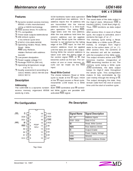
Datasheet4U Logo Datasheet4U.com

UD61466 - DRAM

Datasheet Summary

Description

meanwhile LOW leads to a Write cycle.

Addressing The UD61466 is a dynamic random Both CAS-controlled and W-controlaccess memory organized 65536 led Write cycles are possible with words by 4 bits.

activated RAS signal.

Features

  • UD61466 64K x 4 DRAM SCM facilitates faster data operation with predefined row address. Via 8 address inputs the 16 address bits are transmitted into the internal address memories in a time-multiplex operation. The falling RASedge takes over the row address. After the row address hold time the column address can be applied. During the Read cycle the address transfer is not latched by the falling edge at the CAS input, so that the column address must be applied until the data are valid at the ou.

📥 Download Datasheet

Datasheet preview – UD61466

Datasheet Details

Part number UD61466
Manufacturer ZMD
File Size 200.82 KB
Description DRAM
Datasheet download datasheet UD61466 Datasheet
Additional preview pages of the UD61466 datasheet.
Other Datasheets by ZMD

Full PDF Text Transcription

Click to expand full text
www.DataSheet4U.com Maintenance only Features UD61466 64K x 4 DRAM SCM facilitates faster data operation with predefined row address. Via 8 address inputs the 16 address bits are transmitted into the internal address memories in a time-multiplex operation. The falling RASedge takes over the row address. After the row address hold time the column address can be applied. During the Read cycle the address transfer is not latched by the falling edge at the CAS input, so that the column address must be applied until the data are valid at the output. During Write the column address is taken over with the falling edge of the control signal CAS, or W, that becomes active as the last. The selection of one or more memory circuits can be made via the RAS input.
Published: |