ZPSEMI CJ3404
The CJ3404 use advanced trench technology to provide excellent RDS(ON) and low gate charge. This device is suitable for use as a load switch or in PWM applications.The source leads are separated to allow a Kelvin connection to the source,which may be used to bypass the source inductance.| Part No. | CJ3404 |
|---|---|
| Datasheet | CJ3404 Download |
| Manufacturer | ZPSEMI |
| Description | N-Channel Enhancement Mode Field Effect Transistor |
| Buy | Stock & Price |
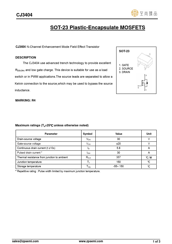
DESCRIPTION
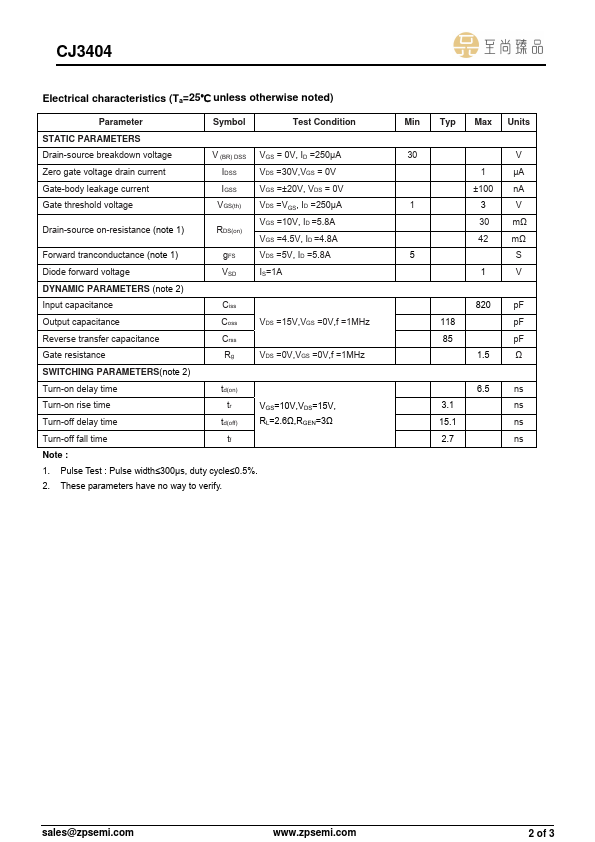
SOT-23 1. GATE 2. SOURCE 3. DRAIN MARKING: R4 Maximum ratings (Ta=25℃ unless otherwise noted) Parameter Symbol Drain-source voltage VDS Gate-source voltage VGS Continuous drain current (t ≤10s) ID Pulsed drain current * IDM Thermal resistance from junction to ambient RθJA Junction temperature TJ Storage temperature Tstg * Repetitive rating : Pulse width limited by maximum junction temperature. Value 30 ±20 5.8 30 357 150 -55~ 150 Unit V V A A ℃/W ℃ ℃ sales@zpsemi.com 1 of 3 CJ3404 Electrical characteristics (Ta=25℃ unless otherwise not