SP8402 Overview
Key Specifications
Max Operating Temp: 125 °C
Min Operating Temp: -55 °C
Key Features
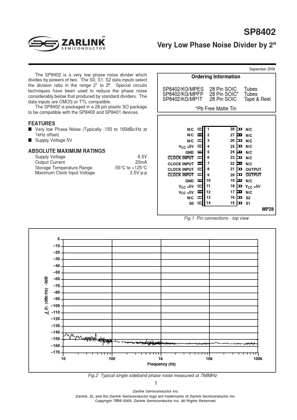
- 170 10 100 1k Frequency (Hz) 10k 100k
| Part | SP8402 |
|---|---|
| Description | Very Low Phase Noise Divider by 2N |
| Manufacturer | Zarlink Semiconductor |
| Size | 489.47 KB |
Max Operating Temp: 125 °C
Min Operating Temp: -55 °C
| Seller | Inventory | Price Breaks | Buy |
|---|---|---|---|
| DigiKey | 2094 | 1+ : 1.89 USD 10+ : 1.305 USD 100+ : 0.8822 USD 500+ : 0.70126 USD |
View Offer |
| DigiKey | 2094 | 1+ : 1.89 USD 10+ : 1.305 USD 100+ : 0.8822 USD 500+ : 0.70126 USD |
View Offer |
| Part Number | Manufacturer | Description |
|---|---|---|
| SP8402 | Mitel Networks | Very Low Phase Noise Divider by 2N |
| SP8402KGMPES | Mitel Networks | Very Low Phase Noise Divider by 2N |
| SP8400KGMPES | Mitel Networks | Very Low Phase Noise Synthesiser Divider |
| SP840S | Eris Technology | Schottky Barrier Rectifiers |
| SP8400 | Mitel Networks | Very Low Phase Noise Synthesiser Divider |