ZVP2120A
ZVP2120A is P-CHANNEL ENHANCEMENT MODE VERTICAL DMOS FET manufactured by Zetex Semiconductors.
FEATURES
- 200 Volt VDS
- RDS(on)=25Ω
ABSOLUTE MAXIMUM RATINGS.
PARAMETER Drain-Source Voltage Continuous Drain Current at Tamb=25°C Pulsed Drain Current Gate Source Voltage Power Dissipation at Tamb=25°C Operating and Storage Temperature Range SYMBOL VDS ID IDM VGS Ptot Tj:Tstg
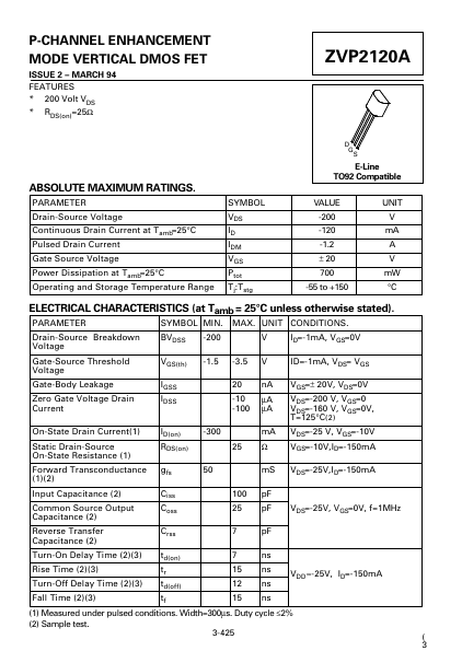
E-Line TO92 patible VALUE -200 -120 -1.2
± 20
UNIT V m A A V m W °C
700 -55 to +150
ELECTRICAL CHARACTERISTICS (at Tamb = 25°C unless otherwise stated).
PARAMETER Drain-Source Breakdown Voltage Gate-Source Threshold Voltage Gate-Body Leakage Zero Gate Voltage Drain Current On-State Drain Current(1) Static Drain-Source On-State Resistance (1) Forward Transconductance (1)(2) Input Capacitance (2) mon Source Output Capacitance (2) Reverse Transfer Capacitance (2) Turn-On Delay Time (2)(3) Rise Time (2)(3) Turn-Off Delay Time (2)(3) Fall Time (2)(3) SYMBOL MIN. BVDSS VGS(th) IGSS IDSS ID(on) RDS(on) gfs Ciss Coss Crss td(on) tr td(off) tf 50 100 25 7 7 15 12 15 -300 25 -200 -1.5 -3.5 20 -10 -100 MAX. UNIT CONDITIONS. V V n A
µA µA
ID=-1m A, VGS=0V ID=-1m A, VDS= VGS VGS=± 20V, VDS=0V VDS=-200 V, VGS=0 VDS=-160 V, VGS=0V, T=125°C(2) VDS=-25 V, VGS=-10V VGS=-10V,ID=-150m A VDS=-25V,ID=-150m A m A
Ω m S p F p F p F ns ns ns ns
VDS=-25V, VGS=0V, f=1MHz
VDD ≈ -25V, ID=-150m A
(1) Measured under pulsed conditions. Width=300µs. Duty cycle ≤2% (2) Sample test. 3-425
( 3
TYPICAL CHARACTERISTICS
ID(On) -On-State Drain Current (Amps) ID(On) -On-State Drain Current (Amps)
VGS= -10V -8V -7V -6V -0.4 -0.4 VGS= -10V -8V -7V -6V
-0.6
-0.3
-5V -0.2 -4.5V -0.1 -4V -3.5V 0 0 -2 -4 -6 -8 -10
-5V -0.2 -4.5V -4V 0 0 -20 -40 -60 -80 -3.5V -100
- Drain Source Voltage (Volts)
- Drain Source Voltage (Volts)
Output Characteristics
Saturation Characteristics
ID(On)-On-State Drain Current (Amps)
-20
VDS-Drain Source Voltage (Volts)
-18 -16 -14 -12 -10 -8 -6 -4 -2 0 0 -2 -4 -6 -8 ID= -300m A -200m A -100m A -50m A -10
VDS= -25V -0.6
-0.4
-10V
-0.2
0 0 -2 -4 -6 -8...