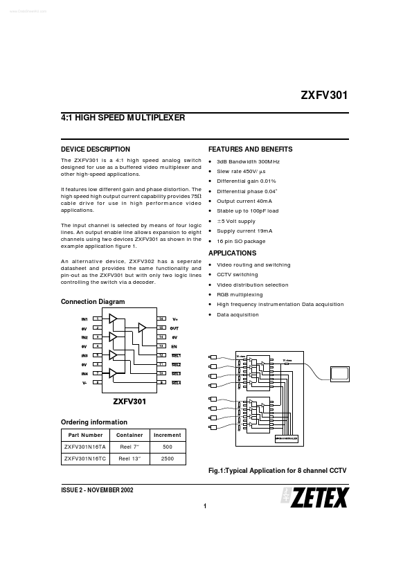
• Part: ZXFV301
  • Description: 4:1 HIGH SPEED MULTIPLEXER
  • Manufacturer: Zetex Semiconductors
  • Size: 307.33 KB
Download ZXFV301 Datasheet PDF
Zetex Semiconductors
ZXFV301
ZXFV301 is 4:1 HIGH SPEED MULTIPLEXER manufactured by Zetex Semiconductors.
DESCRIPTION The ZXFV301 is a 4:1 high speed analog switch designed for use as a buffered video multiplexer and other high-speed applications. It features low different gain and phase distortion. The high speed high output current capability provides 75⍀ cable drive for use in high performance video applications. The input channel is selected by means of four logic lines. An output enable line allows expansion to eight channels using two devices ZXFV301 as shown in the example application figure 1. An alternative device, ZXFV302 has a seperate datasheet and provides the same functionality and pin-out as the ZXFV301 but with only two logic lines controlling the switch via a decoder. FEATURES AND BENEFITS - 3d B Bandwidth 300MHz - Slew rate 450V/ ␮s - Differential gain 0.01% - Differential phase 0.04Њ - Output current 40m A - Stable up to 100p F load - Ϯ5 Volt supply - Supply current 19m A - 16 pin SO package APPLICATIONS - Video routing and switching - CCTV switching - Video distribution selection - RGB multiplexing - High frequency instrumentation Data acquisition - Data acquisition Connection Diagram Ordering information Part Number ZXFV301N16TA ZXFV301N16TC Container Reel 7 ″ Reel 13 ″ Increment 500 2500 Fig.1:Typical Application for 8 channel CCTV ISSUE 2 - NOVEMBER 2002 1 ABSOLUTE MAXIMUM RATINGS Supply voltage VCC Supply voltage VEE Analog inputs to ground Digital inputs to ground Outputs to ground- Output current, max continous Operating Ambient Temperature Range Operating Junction temperature TJMAX -0.5V to +6V -6V to +0.5V VEE -0.5V to VCC +0.5V -0.5V to VCC +0.5V VEE -0.5V to VCC +0.5V 40m A -40ЊC to 85ЊC Storage -65ЊC to 150ЊC 150ЊC- - - - The thermal resistance from the semiconductor die to ambient is typically 120ЊC/W when the SO16 package is mounted on a PCB in free air. The power dissipation of the device when loaded must be designed to keep the device junction temperature below TJMAX. - During power-up and power-down, these voltage ratings...