ZXMP7A17K
ZXMP7A17K is P-channel enhancement mode MOSFET manufactured by Zetex Semiconductors.
Description
This new generation of trench MOSFETs from Zetex utilizes a unique structure that bines the benefits of low on-resistance with fast switching speed. This makes them ideal for high efficiency, low voltage power management applications.
Features
- -
- -
- Low on-resistance Fast switching speed Low threshold Low gate drive DPAK package
Applications
- -
- -
- DC-DC converters Power management functions Disconnect switches Motor control Class D audio output stages
Ordering information
Device ZXMP7A17KTC Reel size (inches) 13 Tape width (mm) 12 Quantity per reel 4,000
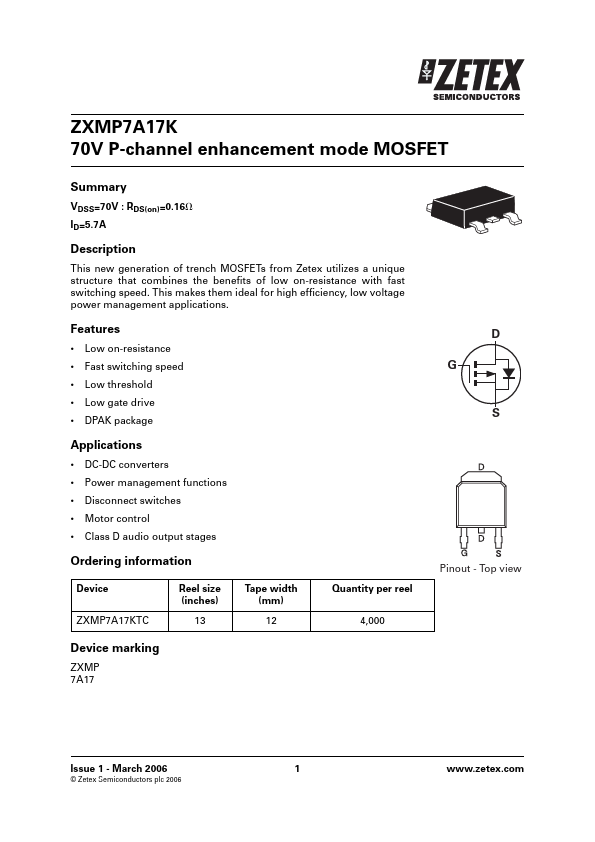
Pinout
- Top view
Device marking
ZXMP 7A17
Issue 1
- March 2006
© Zetex Semiconductors plc 2006
.zetex.
Absolute maximum ratings
Parameter Drain-source voltage Gate-source voltage Continuous drain current @ VGS=10V; TA=25°C (b) @ VGS=10V; TA=25°C (b) @ VGS=10V; TA=25°C (a) Pulsed drain current (c) Continuous source current (body diode) (b) Pulsed source current (body diode) (c) Power dissipation at TA =25°C (a) Linear derating factor Power dissipation at TA =25°C (b) Linear derating factor Power dissipation at TA =25°C (d) Linear derating factor Operating and storage temperature range IDM IS ISM PD Symbol VDSS VGS ID Limit -70 Ϯ20 -5.7 -4.6 -3.8 -17.7 -9.2 -17.7 4.17 33.3 9.25 74 2.11 16.8 -55 to +150 A A A W m W/°C W m W/°C W m W/°C °C Unit V V A
Tj, Tstg
Thermal resistance
Parameter Junction to ambient (a) Junction to ambient (b) Junction to ambient (c) Symbol R⍜JA R⍜JA R⍜JA Limit 30 13.5 59.1 Unit °C/W °C/W °C/W
NOTES: (a) For a device surface mounted on 50mm x 50mm x 1.6mm FR4 PCB with high coverage of single sided 2oz copper, in still air conditions. (b) For a device surface mounted on FR4 PCB measured at t Յ10 sec. (c) Repetitive rating 50mm x 50mm x 1.6mm FR4 PCB, D=0.02 pulse width=300s
- pulse width limited by maximum junction temperature. (d) For a device surface mounted on 25mm x 25mm x 1.6mm FR4 PCB with high coverage of single sided 1oz copper,...