ZXLD1101
ZXLD1101 is ADJUSTABLE LED DRIVER manufactured by Zetex Semiconductors.
DESCRIPTION
The ZXLD1101 is a PFM inductive boost converter designed for driving 2, 3 or 4 series connected white LEDs from a Li-Ion cell and up to 8 LEDs from a 5V supply. The device operates from an input supply of between 2.5V and 5.5V and provides an adjustable output current of up to 50m A. The ZXLD1101 includes the output switch and peak current sense resistor, and can operate with a maximum output voltage of 28V. Quiescent current is typically 60A and a shutdown function is provided to reduce this current to less than 500n A in the 'off' state. Output current can be adjusted by applying a PWM control signal to the 'Enable' pin. Depending upon the control frequency, this will provide either a continuous or a 'chopped' output current. The PWM filter ponents are contained within the chip. The device is assembled in the TSOT23-5 pin package with 1mm maximum height profile.
ADVANCED FEATURES
- True Analog Dimming via PWM
APPLICATIONS
- Mobile phones
- Digital cameras
- PDAs
- LCD modules
- Portable internet appliances
- Palmtop puters
FEATURES
- -
- -
- -
- -
- -
1mm height profile TSOT23-5 pin package Internal PWM filter for flicker free output High efficiency (80% typ) Wide input voltage range: 2.5V to 5.5V Up to 50m A output current Low quiescent current: (60A typ) 500n A maximum shutdown current Up to 1MHz switching frequency Low external ponent count Inherently matched LED currents
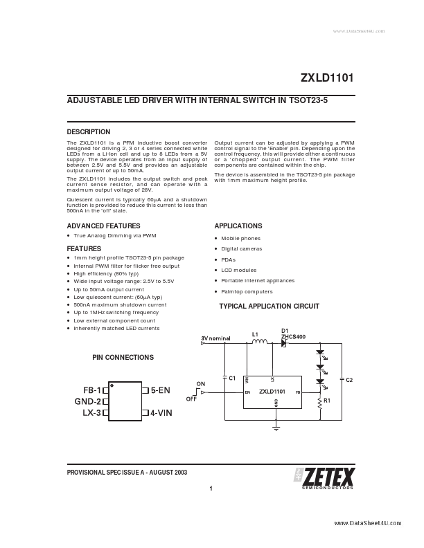
TYPICAL APPLICATION CIRCUIT
PIN CONNECTIONS
PROVISIONAL SPEC ISSUE A
- AUGUST 2003 1
SEMICONDUCTORS
..
ORDERING INFORMATION
DEVICE ZXLD1101ET5 DEVICE DESCRIPTION
Boost converter in TSOT23-5 TEMPERATURE RANGE -40°C to +85°C PART MARK 1101 TAPING OPTIONS TA, TC
ZXLD1101ET5TA for 7” reel of 3,000 devices ZXLD1101ET5TA for 13” reel of 10,000 devices
ABSOLUTE MAXIMUM RATINGS (Voltages to GND unless otherwise stated)
PARAMETER Input voltage LX output voltage Switch output current Power dissipation Operating temperature Storage temperature Junction temperature SYMBOL (V...