GENERAL DESCRIPTION
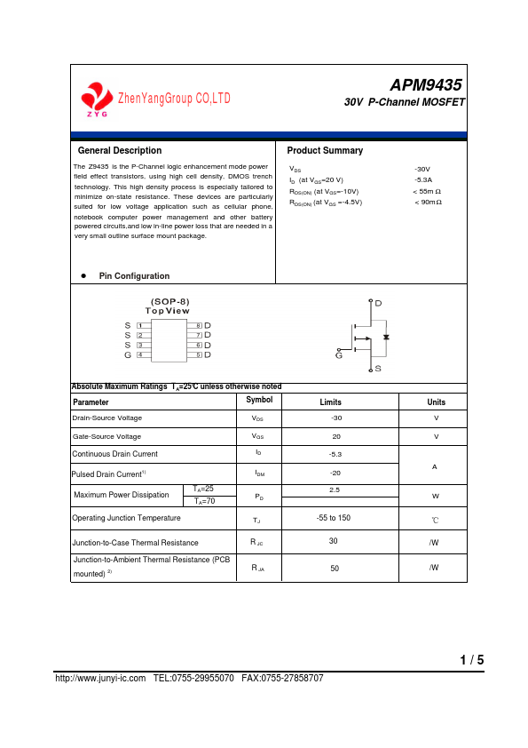
These devices are particularly suited for low voltage application such as cellular phone, notebook computer power management and other battery powered circuits,and low in-line power loss that are needed in a very small outline surface mount package. Product Summary VDS ID (at VGS=20 V) RDS(ON) (at VGS=-10V) RDS(ON) (at VGS =-4.5V) z Pin Configuration -30V -5.3A < 55m Ω < 90mΩ ABSOLUTE MAXIMUM RATINGS
TA=25°C unless otherwise noted Parameter Symbol Drain-Source Voltage VDS Gate-Source Voltage Continuous Drain Current VGS ID Pulsed Drain Current1) Maximum Power Dissipation Operating Junction Temperature TA=25 TA=70 IDM PD TJ Junction-to-Case Thermal Resistance Junction-to-Ambient Thermal Resistance (PCB mounted) 2) R JC R JA Limits -30 20 -5.3 -20 2.5 -55 to 150 30 50 Units Units V V A W ℃ /W /W TEL:0755-29955070 FAX:0755-27858707 1/5 ZhenYangGroup CO,LTD APM9435 z ELECTRICAL CHARACTERISTICS
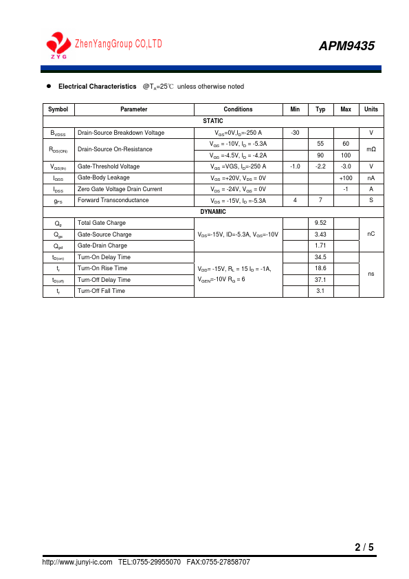
@TA=25℃ unless otherwise noted Symbol Parameter BVB DSS Drain-Source Breakdow...