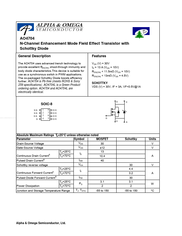
GENERAL DESCRIPTION
AO4704L is a Green Product ordering option. AO4704 and AO4704L are electrically identical. FEATURES
VDS (V) = 30V ID = 13 A (VGS = 10V) RDS(ON) < 11.5mΩ (VGS = 10V) RDS(ON) < 13mΩ (VGS = 4.5V) SCHOTTKY VDS (V) = 30V, IF = 3A, VF<0.5V@1A SOIC-8 S/A S/A S/A G 1 2 3 4 8 7 6 5 D/K D/K D/K D/K D K G S A ABSOLUTE MAXIMUM RATINGS
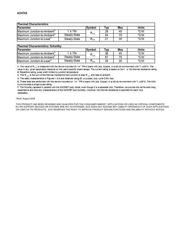
T A=25°C unless otherwise noted Symbol Parameter MOSFET V DS Drain-Source Voltage 30 VGS Gate-Source Voltage ±12 TA=25°C 13 ID Continuous Drain CurrentA TA=70°C 10.4 IDM Pulsed Drain Current B 40 V Schottky reverse voltage KA Continuous Forward CurrentA Pulsed Diode Forward Current Power Dissipation B Schottky Units V V A TA=25°C TA=70°C TA=25°C TA=70°C IF IFM PD TJ, TSTG 3.1 2 -55 to 150 30 4.4 3.2 30 3.1 2 -55 to 150 V A W °C Junction and Storage Temperature Range Alpha & Omega Semiconductor, Ltd. AO4704 Thermal Characteristics Parameter A Maximum Junction-to-Ambient A Maximum Junction-to-Ambient C Maximum Junction-to-Lead Thermal Characteristic... Alpha & Omega Semiconductors