Alpha & Omega Semiconductors AOI206
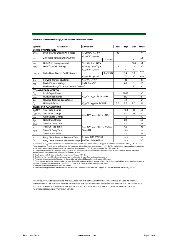
The value of RθJA is measured with the device mounted on 1in2 FR-4 board with 2oz. The Power dissipation PDSM is based on R θJA and the maximum allowed junction temperature of 150°C.| Part No. | AOI206 |
|---|---|
| Datasheet | AOI206 Download |
| Manufacturer |  Alpha & Omega Semiconductors |
| Description | 30V N-Channel MOSFET |
| Buy | Stock & Price |
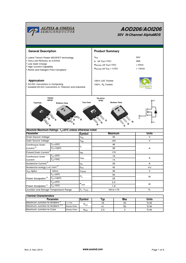
GENERAL DESCRIPTION
● Latest Trench Power MOSFET technology● Very Low RDS(on) at 4.5VGS
● Low Gate Charge
● High Current Capability
● RoHS and Halogen-Free Compliant Product Summary VDS ID (at VGS=10V) RDS(ON) (at VGS=10V) RDS(ON) (at VGS = 4.5V) Application
● DC/DC Converters in Computing
● Isolated DC/DC Converters in Telecom and Industrial 100% UIS Tested 100% Rg Tested 30V 46A < 5mΩ < 10mΩ TopView TO252 DPAK Bottom View Top View TO-251A IPAK Bottom View D D DS G DG S S D G G G D S
ABSOLUTE MAXIMUM RATINGS
TA=25°C unless otherwise noted Parameter Symbol Drain-Source Voltage VDS Gate-Source Voltage VGS Continuous Drain Current G TC=25°C TC=100°C ID Pulsed Drain Current C IDM Continuous Drain Current TA=25°C TA=70°C IDSM Avalanche Current C IAS Avalanche energy L=0.1mH C EAS VDS Spike 100ns VSPIKE TC=25°C Power Dissipation B TC=100°C PD TA=25°C Power Dissipation A TA=70°C PDSM Junction and Storage Temperature Range TJ, TSTG Maximum 30 ±20 46 36 170 18 14 29 42 36 50 25 2.5 1.6 -55 to...