Alpha & Omega Semiconductors AOT2610L
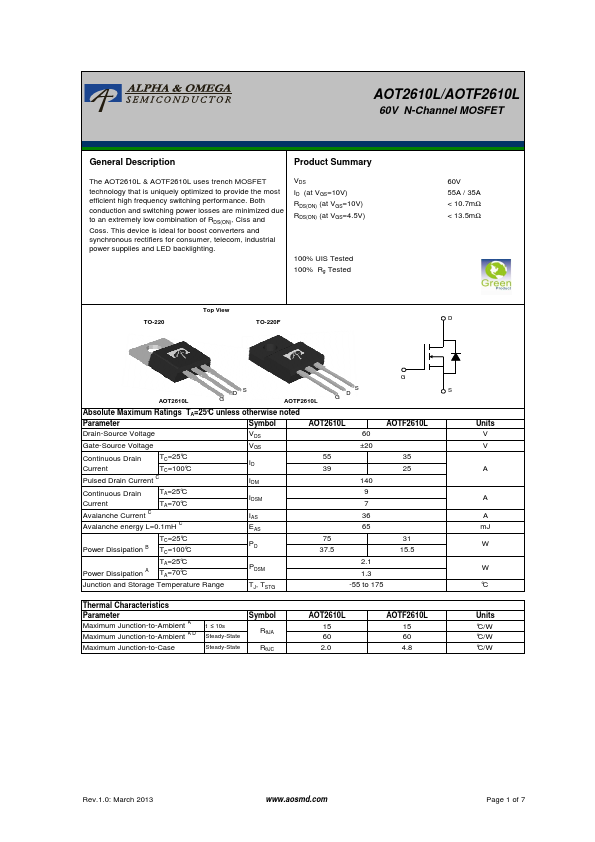
The AOT2610L & AOTF2610L uses trench MOSFET technology that is uniquely optimized to provide the most efficient high frequency switching performance. Both conduction and switching power losses are minimized due to an extremely low combination of RDS(ON), Ciss and Coss. This device is ideal for boost converters and synchronous rectifiers for consumer, telecom, industrial power supplies and LED backlighting.| Part No. | AOT2610L |
|---|---|
| Datasheet | AOT2610L Download |
| Manufacturer |  Alpha & Omega Semiconductors |
| Description | N-Channel MOSFET |
| Buy | Stock & Price |
GENERAL DESCRIPTION
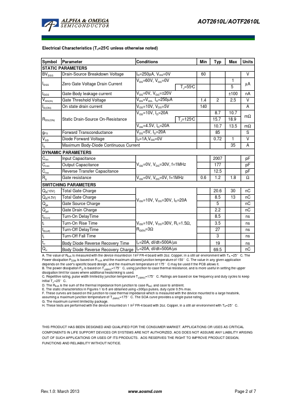
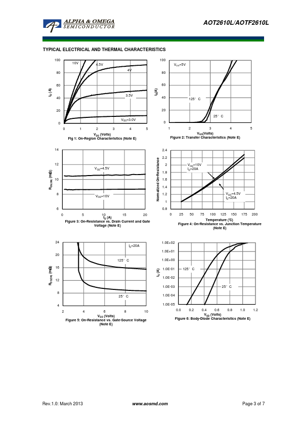
Product Summary VDS ID (at VGS=10V) RDS(ON) (at VGS=10V) RDS(ON) (at VGS=4.5V) 100% UIS Tested 100% Rg Tested TO-220 Top View TO-220F 60V 55A / 35A < 10.7mΩ < 13.5mΩ D G AOT2610L DS G AOTF2610L S GD SABSOLUTE MAXIMUM RATINGS
TA=25°C unless otherwise noted Parameter Symbol Drain-Source Voltage VDS Gate-Source Voltage VGS Continuous Drain Current TC=25°C TC=100°C ID Pulsed Drain Current C IDM Continuous Drain Current TA=25°C TA=70°C IDSM Avalanche Current C IAS Avalanche energy L=0.1mH C EAS TC=25°C Power Dissipation B TC=100°C PD TA=25°C Power Dissipation A TA=70°C PDSM Junction and Storage Temperature Range TJ, TSTG AOT2610L AOTF2610L 60 ±20 55 35 39 25 140 9 7 36 65 75 31 37.5 15.5 2.1 1.3 -55 to 175 Thermal Characteristics Parameter Maximum Junction-to-Ambient A Maximum Junction-to-Ambient A D Maximum Junction-to-Case t ≤ 10s Steady-State Steady-State Symbol RθJA RθJC AOT2610L 15 60 2.0 AOTF2610L 15 60 4.8 Units V V A A A mJ W W °C Units °C/W °C/W °C/W Rev.1.0: M...