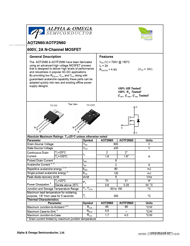
GENERAL DESCRIPTION
FEATURES
VDS (V) = 700V @ 150°C ID = 2A RDS(ON) < 4.4Ω (VGS = 10V) 100% UIS Tested! 100% R g Tested! C iss , C oss , C rss Tested! TO-220 Top View TO-220F D G D G S D G S S ABSOLUTE MAXIMUM RATINGS
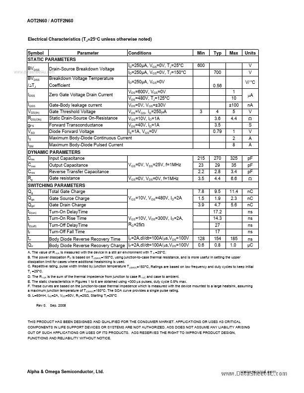
TA=25°C unless otherwise noted AOT2N60 Parameter AOTF2N60 Symbol VDS Drain-Source Voltage 600 VGS ±30 Gate-Source Voltage Continuous Drain Current Pulsed Drain Current C Units V V A A mJ mJ V/ns W W/ oC °C °C TC=25°C TC=100°C ID IDM IAR EAR EAS dv/dt PD TJ, TSTG TL 2 1.6 8 2 60 120 5 74 0.6 -50 to 150 300 AOT2N60 65 0.5 1.7 2* 1.6* Avalanche Current C, G Repetitive avalanche energy C, G Single pulsed avalanche energy G Peak diode recovery dv/dt TC=25°C B Power Dissipation Derate above 25oC Junction and Storage Temperature Range Maximum lead temperature for soldering purpose, 1/8" from case for 5 seconds Thermal Characteristics Parameter Maximum Junction-to-Ambient A,D 31 0.25 Symbol RθJA A R θCS Maximum Case-to-Sink RθJC Maximum Junction-to-Case * Drain current limited by maximum junction temperature. Alpha & Omega Semiconductors