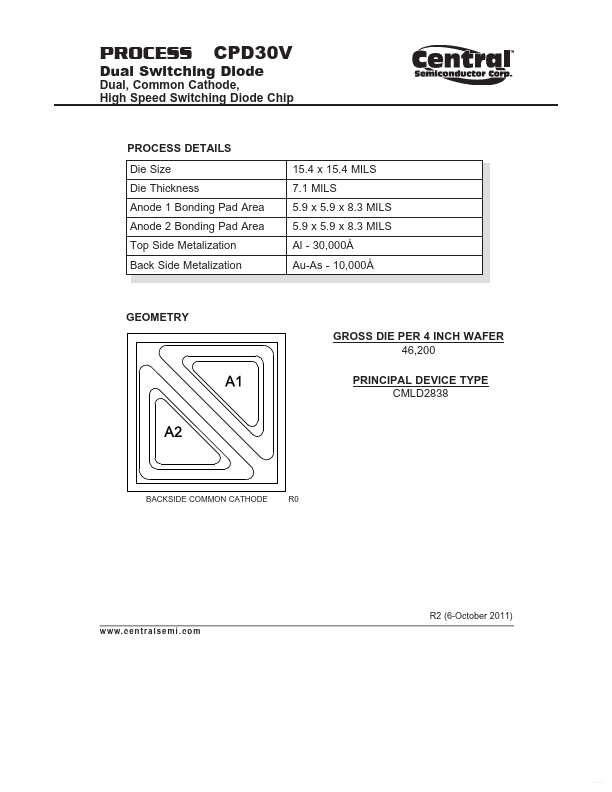
CPD30V Description
PROCESS CPD30V Typical R2 (6-October 2011) w w.
CPD30V Key Features
- s e m i . c o m http://.. PROCESS CPD30V Typical
CPD30V is High Speed Switching Diode manufactured by centralsemi.
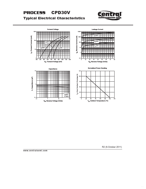
PROCESS CPD30V Typical R2 (6-October 2011) w w.