Texas Instruments 54HC112
The ’HC112 devices contain two independent J-K negative-edge-triggered flip-flops. When PRE and CLR are inactive (high), data at the J and K inputs meeting the setup time requirements are transferred to the outputs on the negative-going edge of the clock (CLK) pulse.| Part No. | 54HC112 |
|---|---|
| Datasheet | 54HC112 Download |
| Manufacturer |  Texas Instruments |
| Description | Dual J-K Negative-Edge-Triggered Flip-Flops |
| Buy | Stock & Price |

FEATURES
● Wide operating voltage range of 2 V to 6 V● Outputs can drive up to 10 LSTTL loads
● Low power consumption, 40-μA max ICC
● Typical tpd = 13 ns
● ±4-mA output drive at 5 V
● Low input current of 1 μA max 2
DESCRIPTION
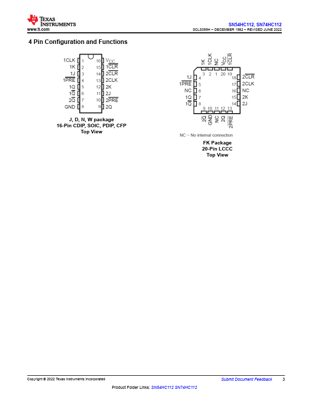
A low level at the preset (PRE) or clear (CLR) inputs sets or resets the outputs, regardless of the levels of the other inputs. Clock triggering occurs at a voltage level and is not directly related to the fall time of the CLK pulse. Following the hold-time interval, data at the J and K inputs may be changed without affecting the levels at the outputs. These versatile flipflops perform as toggle flip-flops by tying J and K high. PART NUMBER SN54HC112J SN74HC112D SN74HC112N SN54HC112FK SN54HC112W Device Information PACKAGE(1) BODY SIZE (NOM) CDIP (16) 24.38 mm × 6.92 mm SOIC (16) 9.90 mm × 3.90 mm PDIP (16) 19.31 mm × 6.35 mm LCCC (20) 8.89 mm × 8.45 mm CFP (16) 10.16 mm × 6.73 mm (1) For all available packages, see the orderable addendum at the end of the data sheet.