Texas Instruments 74ACT11181
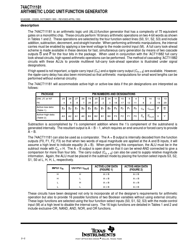
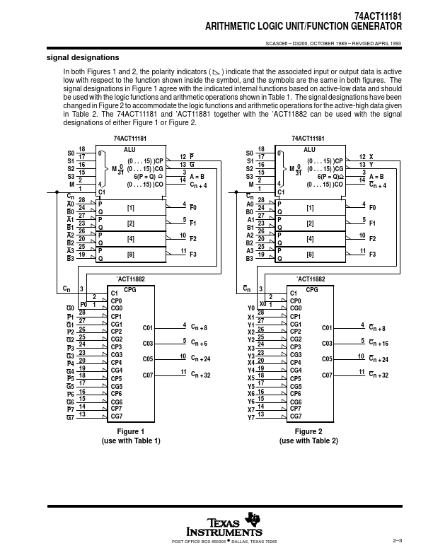
The 74ACT11181 is an arithmetic logic unit (ALU)/function generator that has a complexity of 75 equivalent gates on a monolithic chip. These circuits perform 16 binary arithmetic operations on two 4-bit words as shown in Tables 1 and 2. These operations are selected by the four function-select lines (S0, S1, S2, S3) and include addition, subtraction, decrement, and straight transfer.| Part No. | 74ACT11181 |
|---|---|
| Datasheet | 74ACT11181 Download |
| Manufacturer |  Texas Instruments |
| Description | ARITHMETIC LOGIC UNIT/FUNCTION GENERATOR |
| Buy | Stock & Price |
74ACT11181 ARITHMETIC LOGIC UNIT/FUNCTION GENERATOR
● Inputs Are TTL-Voltage Compatible
● New Flow-Through Architecture Optimizes PCB Layout
● Center-Pin VCC and GND Configurations Minimize High-Speed Switching Noise t● EPIC (Enhanced-Performance Implanted CMOS) 1-mm Process
● 500-mA Typical Latch-Up Immunity at 125°C
● Full Look Ahead for High-Speed Operations on Long Words
● Arithmetic Operating Modes: Addition Subtraction Shift Operand A One Position Magnitude Comparison Plus Twelve Other Arithmetic Operations
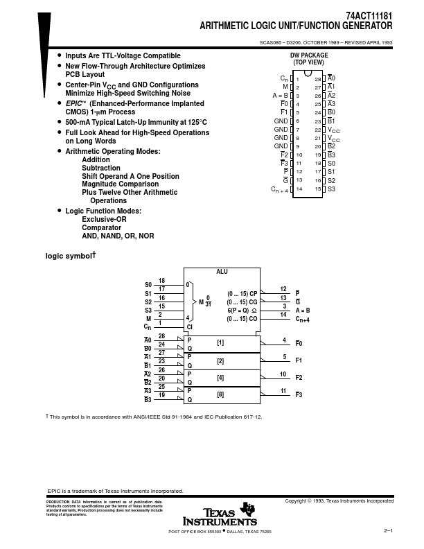
● Logic Function Modes: Exclusive-OR Comparator AND, NAND, OR, NOR SCAS086 – D3200, OCTOBER 1989 – REVISED APRIL 1993 DW PACKAGE (TOP VIEW) Cn M A=B F0 F1 GND GND GND GND F2 F3 P G Cn + 4 1 2 3 4 5 6 7 8 9 10 11 12 13 14 28 A0 27 A1 26 A2 25 A3 24 B0 23 B1 22 VCC 21 VCC 20 B2 19 B3 18 S0 17 S1 16 S2 15 S3 logic symbol† 18 S0 17 S1 16 S2 15 S3 2 M Cn 1 28 A0 24 B0 27 A1 23 B1 26 A2 20 B2 25 A3 19 B3 ALU 0 0 M 31 4 CI (0 ... 15) CP (0 ... 15) CG 6(P = Q) (0 ... 15) CO P [1] Q P [2] Q P [4] Q P [8] Q † This symbol is in accordance with ANSI/IEEE Std 91-1984 and IEC Publication 617-12.