74ACT11240
74ACT11240 is OCTAL BUFFER/LINE DRIVER manufactured by Texas Instruments.
D Inputs Are TTL-Voltage patible D Flow-Through Architecture Optimizes
PCB Layout
D Center-Pin VCC and GND Configurations
Minimize High-Speed Switching Noise
D EPICt (Enhanced-Performance Implanted
CMOS) 1-mm Process
D 500-mA Typical Latch-Up Immunity at
125°C
D Package Options Include Plastic
Small-Outline (DW) and Shrink Small-Outline (DB) Packages, and Standard Plastic 300-mil DIPs (NT) description
74ACT11240 OCTAL BUFFER/LINE DRIVER
WITH 3-STATE OUTPUTS
SCAS210A
- MAY 1987
- REVISED APRIL 1996
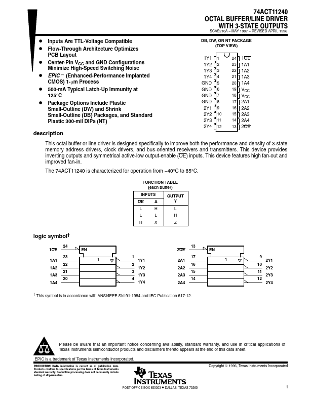
DB, DW, OR NT PACKAGE (TOP VIEW)
1Y1 1 1Y2 2 1Y3 3 1Y4 4 GND 5 GND 6 GND 7 GND 8 2Y1 9 2Y2 10 2Y3 11 2Y4 12
24 1OE 23 1A1 22 1A2 21 1A3 20 1A4 19 VCC 18 VCC 17 2A1 16 2A2 15 2A3 14 2A4 13...