APPLICATIONS
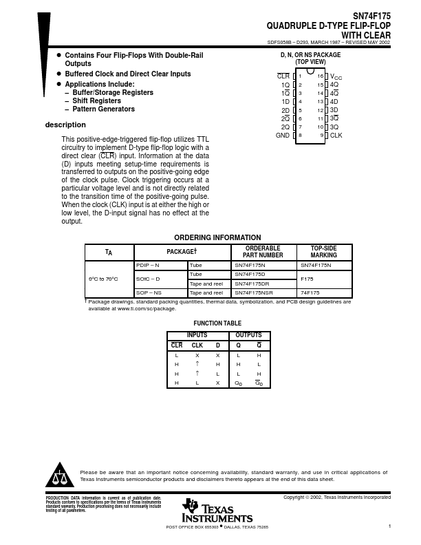
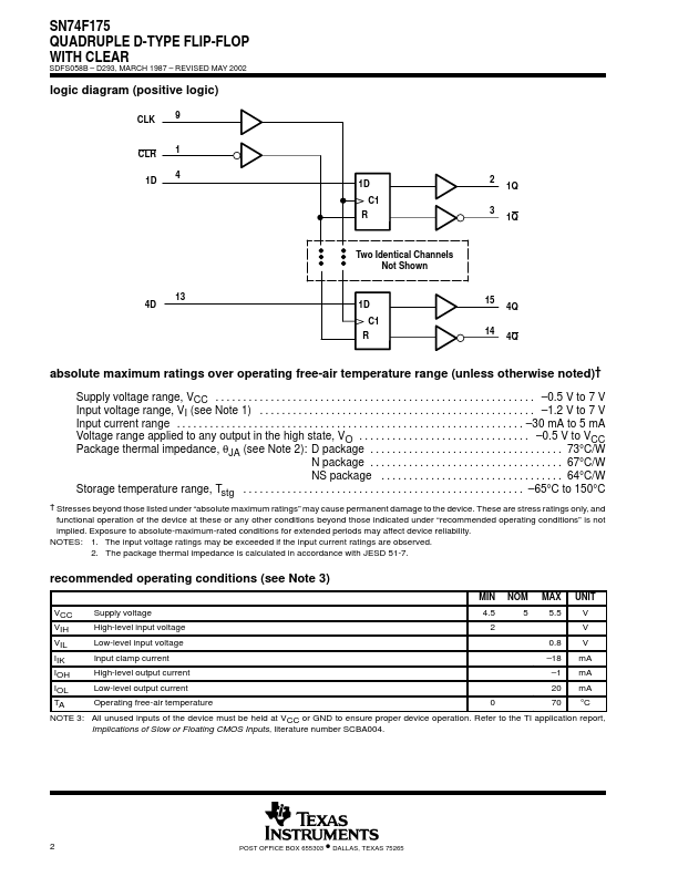
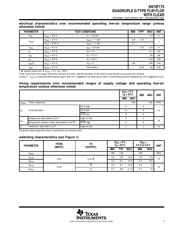
Include: – Buffer/Storage Registers – Shift Registers – Pattern Generators description Information at the data (D) inputs meeting setup-time requirements is transferred to outputs on the positive-going edge of the clock pulse. Clock triggering occurs at a particular voltage level and is not directly related to the transition time of the positive-going pulse. SN74F175 QUADRUPLE D-TYPE FLIP-FLOP WITH CLEAR SDFS058B – D293, MARCH 1987 – REVISED MAY 2002 D, N, OR NS PACKAGE (TOP VIEW) CLR 1 1Q 2 1Q 3 1D 4 2D 5 2Q 6 2Q 7 GND 8 16 VCC 15 4Q 14 4Q 13 4D 12 3D 11 3Q 10 3Q 9 CLK ORDERING INFORMATION TA PACKAGE† ORDERABLE PART NUMBER TOP-SIDE MARKING PDIP – N Tube SN74F175N SN74F175N 0°C to 70°C SOIC – D Tube Tape and reel SN74F175D SN74F175DR F175 SOP – NS Tape and reel SN74F175NSR 74F175 † Package drawings, standard packing quantities, thermal data, symbolization, and PCB design guidelines are available at FUNCTION TABLE INPUTS CLR CLK D L X X H ↑ H H ↑ L H L X OUTPUTS Q Q L H H L... Texas Instruments