APPLICATIONS
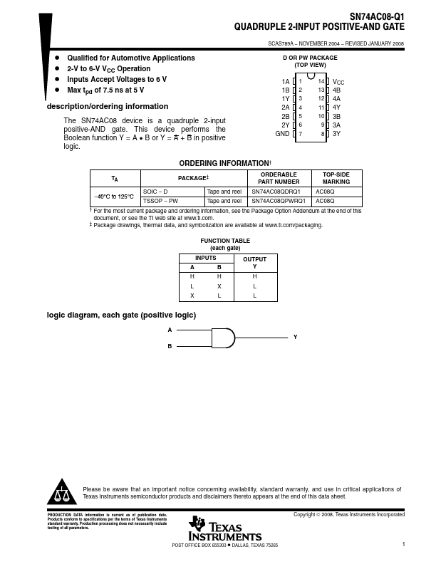
D 2-V to 6-V VCC Operation D Inputs Accept Voltages to 6 V D Max tpd of 7.5 ns at 5 V description/ordering information SCAS789A − NOVEMBER 2004 − REVISED JANUARY 2008 D OR PW PACKAGE (TOP VIEW) 1A 1 1B 2 1Y 3 2A 4 2B 5 2Y 6 GND 7 14 VCC 13 4B 12 4A 11 4Y 10 3B 9 3A 8 3Y ORDERING INFORMATION† TA PACKAGE‡ ORDERABLE PART NUMBER TOP-SIDE MARKING SOIC − D −40°C to 125°C TSSOP − PW Tape and reel Tape and reel SN74AC08QDRQ1 SN74AC08QPWRQ1 AC08Q AC08Q † For the most current package and ordering information, see the Package Option Addendum at the end of this document, or see the TI web site at ‡ Package drawings, thermal data, and symbolization are available at FUNCTION TABLE (each gate) INPUTS A B OUTPUT Y H H H L X L X L L logic diagram, each gate (positive logic) A Y B Please be aware that an important notice concerning availability, standard warranty, and use in critical applications of Texas Instruments semiconductor products and disclaimers thereto appears at the end of this data sheet. Texas Instruments