Texas Instruments ADC08161
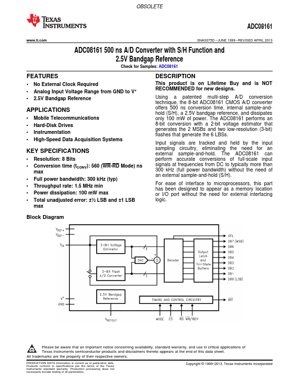
The ADC08161 performs an 8-bit conversion with a 2-bit voltage estimator that generates the 2 MSBs and two low-resolution (3-bit) flashes that generate the 6 LBSs. The ADC08161 can perform accurate conversions of full-scale input signals at frequencies from DC to typically more than 300 kHz (full power bandwidth) without the need of an external sample-and-hold (S/H). For ease of interface to microprocessors, this part has been designed to appear as a memory location or I/O port without the need for external interfacing logic.| Part No. | ADC08161 |
|---|---|
| Datasheet | ADC08161 Download |
| Manufacturer |  Texas Instruments |
| Description | A/D Converter |
| Buy | Stock & Price |
FEATURES
1●2 No External Clock Required
● Analog Input Voltage Range from GND to V+
● 2.5V Bandgap Reference
APPLICATIONS
● Mobile Telecommunications● Hard-Disk Drives
● Instrumentation
● High-Speed Data Acquisition Systems KEY SPECIFICATIONS
● Resolution: 8 Bits
● Conversion time (tCONV): 560 (WR-RD Mode) ns max
● Full power bandwidth: 300 kHz (typ)
● Throughput rate: 1.5 MHz min
● Power dissipation: 100 mW max
● Total unadjusted error: ±½ LSB and ±1 LSB max
DESCRIPTION
This product is on Lifetime Buy and is NOT RECOMMENDED for new designs. Using a patented multi-step A/D conversion technique, the 8-bit ADC08161 CMOS A/D converter offers 500 ns conversion time, internal sample-andhold (S/H), a 2.5V bandgap reference, and dissipates only 100 mW of power. Input signals are tracked and held by the input sampling circuitry, eliminating the need for an external sample-and-hold. Block Diagram 1 Please be aware that an important notice concerning availability, standard warranty, and use in critical applications of Texas Instruments semiconductor products and disclaimers thereto appears at the end of this data sheet.