Texas Instruments ADC12062
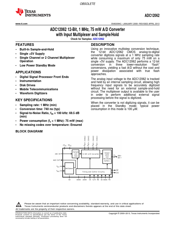
The ADC12062 performs a 12-bit conversion in three lower-resolution “flash” conversions, yielding a fast A/D without the cost and power dissipation associated with true flash approaches. The analog input voltage to the ADC12062 is tracked and held by an internal sampling circuit, allowing high frequency input signals to be accurately digitized without the need for an external sample-and-hold circuit. The multiplexer output is available to the user in order to perform additional external signal processing before the signal is digitized.| Part No. | ADC12062 |
|---|---|
| Datasheet | ADC12062 Download |
| Manufacturer |  Texas Instruments |
| Description | A/D Converter |
| Buy | Stock & Price |
FEATURES
1●2 Built-In Sample-and-Hold
● Single +5V Supply
● Single Channel or 2 Channel Multiplexer Operation
● Low Power Standby Mode
APPLICATIONS
● Digital Signal Processor Front Ends● Instrumentation
● Disk Drives
● Mobile Telecommunications
● Waveform Digitizers KEY SPECIFICATIONS
● Sampling rate: 1 MHz (min)
● Conversion time: 740 ns (typ)
● Signal-to-Noise Ratio, fIN = 100 kHz: 69.5 dB (min)
● Power consumption (fs = 1 MHz): 75 mW (max)
● No missing codes over temperature: Ensured
DESCRIPTION
Using an innovative multistep conversion technique, the 12-bit ADC12062 CMOS analog-to-digital converter digitizes signals at a 1 MHz sampling rate while consuming a maximum of only 75 mW on a single +5V supply. When the converter is not digitizing signals, it can be placed in the Standby mode; typical power consumption in this mode is 100 μW. BLOCK DIAGRAM 1 Please be aware that an important notice concerning availability, standard warranty, and use in critical applications of Texas Instruments semiconductor products and disclaimers thereto appears at the end of this data sheet.