ADS42LB69
ADS42LB69 is Analog-to-Digital Converter manufactured by Texas Instruments.
- Part of the ADS42LB49 comparator family.
- Part of the ADS42LB49 comparator family.
Product Folder
Sample & Buy
Technical Documents
Tools & Software
Support & munity
ADS42LB49, ADS42LB69
SLAS904F
- OCTOBER 2012
- REVISED MAY 2016
ADS42LBx9 14- and 16-Bit, 250-MSPS, Analog-to-Digital Converters
1 Features
- 1 Dual Channel
- 14- and 16-Bit Resolution
- Maximum Clock Rate: 250 MSPS
- Analog Input Buffer with High Impedance Input
- Flexible Input Clock Buffer with
Divide-by-1, -2, and -4
- 2-VPP and 2.5-VPP Differential Full-Scale Input
(SPI-Programmable)
- DDR or QDR LVDS Interface
- 64-Pin VQFN Package (9-mm × 9-mm)
- Power Dissipation: 820 m W/ch
- Aperture Jitter: 85 f S
- Internal Dither
- Channel Isolation: 100 d B
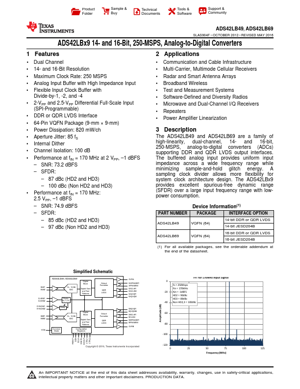
- Performance at f IN = 170 MHz at 2 VPP,
- 1 d BFS
- SNR: 73.2 d BFS
- SFDR:
- 87 d Bc (HD2 and...