CD4021B-Q1
Description
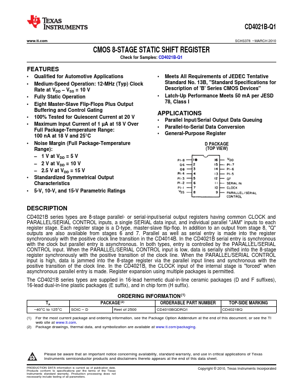
CD4021B series types are 8-stage parallel- or serial-input/serial output registers having mon CLOCK and PARALLEL/SERIAL CONTROL inputs, a single SERIAL data input, and individual parallel "JAM" inputs to each register stage.
Key Features
- Qualified for Automotive Applications
- Medium-Speed Operation: 12-MHz (Typ) Clock Rate at VDD - VSS = 10 V
- Fully Static Operation
- Eight Master-Slave Flip-Flops Plus Output Buffering and Control Gating
- 100% Tested for Quiescent Current at 20 V
- Maximum Input Current of 1 µA at 18 V Over Full Package-Temperature Range: 100 nA at 18 V and 25°C
- Noise Margin (Full Package-Temperature Range): - 1 V at VDD = 5 V - 2 V at VDD = 10 V - 2.5 V at VDD = 15 V
- Standardized Symmetrical Output Characteristics
- Meets All Requirements of JEDEC Tentative Standard No. 13B, "Standard Specifications for Description of 'B' Series CMOS Devices"
- Latch-Up Performance Meets 50 mA per JESD 78, Class I
Applications
- Parallel-to-Serial Data Conversion