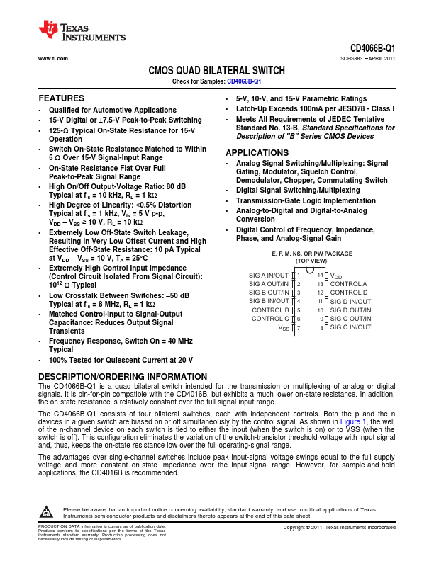
CD4066BQ
Key Features
- Qualified for Automotive Applications
- 15-V Digital or ±7.5-V Peak-to-Peak Switching
- 125-Ω Typical On-State Resistance for 15-V Operation
- Switch On-State Resistance Matched to Within 5 Ω Over 15-V Signal-Input Range
- On-State Resistance Flat Over Full Peak-to-Peak Signal Range
- High On/Off Output-Voltage Ratio: 80 dB Typical at fis = 10 kHz, RL = 1 kΩ
- High Degree of Linearity: <0.5% Distortion Typical at fis = 1 kHz, Vis = 5 V p-p, VDD - VSS ≥ 10 V, RL = 10 kΩ
- Extremely High Control Input Impedance (Control Circuit Isolated From Signal Circuit): 1012 Ω Typical
- Low Crosstalk Between Switches: -50 dB Typical at fis = 8 MHz, RL = 1 kΩ
- Matched Control-Input to Signal-Output Capacitance: Reduces Output Signal Transients