CD54HC299
Features
- Buffered Inputs
- Four Operating Modes: Shift Left, Shift Right, Load and Store
- Can be Cascaded for N-Bit Word Lengths
- I/O0
- I/O7 Bus Drive Capability and Three-State for Bus Oriented Applications
- Typical f MAX = 50MHz at VCC = 5V, CL = 15p F, TA = 25o C
- Fanout (Over Temperature Range)
- Standard Outputs
- -
- 10 LSTTL Loads
- Bus Driver Outputs
- - . . . 15 LSTTL Loads
- Wide Operating Temperature Range . . . -55o C to 125o C
- Balanced Propagation Delay and Transition Times
- Significant Power Reduction pared to LSTTL Logic ICs
- HC Types
- 2V to 6V Operation
- High Noise Immunity: NIL = 30%, NIH = 30% of VCC at VCC = 5V
- HCT Types
- 4.5V to 5.5V Operation
- Direct LSTTL Input Logic patibility, VIL= 0.8V (Max), VIH = 2V (Min)
- CMOS Input patibility, Il ≤ 1µA at VOL, VOH
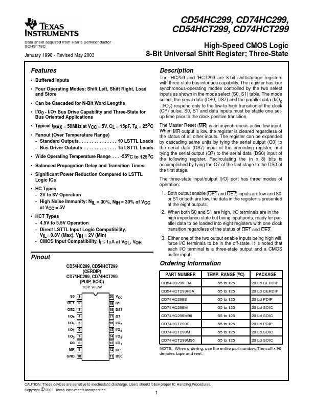
Pinout
CD54HC299, CD54HCT299 (CERDIP)
CD74HC299, CD74HCT299 (PDIP, SOIC) TOP VIEW
S0 1 OE1 2 OE2 3 I/O6 4 I/O4 5 I/O2 6 I/O0 7
Q0 8 MR 9 GND 10
20 VCC 19 S1...