CD54HC4511
Features
- 2-V to 6-V VCC operation ('HC4511)
- 4.5-V to 5.5-V VCC operation (CD74HCT4511)
- High-output sourcing capability
- 7.5 m A at 4.5 V (CD74HCT4511)
- 10 m A at 6 V ('HC4511)
- Input latches for BCD code storage
- Lamp test and blanking capability
- Balanced propagation delays and transition times
- Significant power reduction pared to LSTTL logic IC's
- 'HC4511
- High noise immunity, NIL or NIH = 30% of VCC at VCC = 5 V
- CD74HCT4511
- Direct LSTTL input logic patibility, VIL = 0.8 V Maximum, VIH = 2 V minimum
- CMOS input patibility, II ≤ 1μA at VOL, VOH
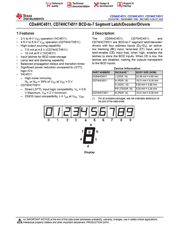
2 Description
The
CD54HC4511,
CD74HC4511, and
CD74HCT4511 are BCD-to-7 segment latch/decoder/ drivers with four address inputs (D0- D3), an activelow blanking (BL) input, lamp-test (LT) input, and a latch-enable (LE) input that, when high, enables the latches to store the BCD inputs. When LE is low, the latches are disabled, making the outputs transparent to the BCD inputs.
PART NUMBER CD54HC4511 CD74HC4511
CD74HCT4...