CD54HCT10
CD54HCT10 is Triple 3-Input NAND Gates manufactured by Texas Instruments.
CDx4HCT10 Triple 3-Input NAND Gates
CD74HCT10, CD54HCT10
SCHS404
- JUNE 2020
1 Features
- LSTTL input logic patible
- VIL(max) = 0.8 V, VIH(min) = 2 V
- CMOS input logic patible
- II ≤ 1 µA at VOL, VOH
- Buffered inputs
- 4.5 V to 5.5 V operation
- Wide operating temperature range:
-55°C to +125°C
- Supports fanout up to 10 LSTTL loads
- Significant power reduction pared to LSTTL logic ICs
2 Applications
- Alarm / tamper detect circuit
- S-R latch
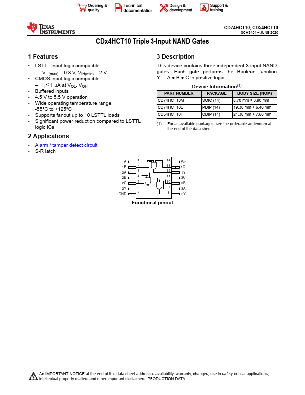
3 Description
This device contains three independent 3-input NAND gates. Each gate performs the Boolean function Y = A
- B
- C in positive logic.
Device Information(1)
PART NUMBER
PACKAGE
BODY SIZE (NOM)
CD74HCT10M
SOIC...