CD54HCT20F
CD54HCT20F is Dual 4-Input NAND Gates manufactured by Texas Instruments.
- Part of the CD54HCT20 comparator family.
- Part of the CD54HCT20 comparator family.
CDx4HCT20 Dual 4-Input NAND Gates
CD74HCT20, CD54HCT20
SCHS417
- JUNE 2020
1 Features
3 Description
- LSTTL input logic patible
- VIL(max) = 0.8 V, VIH(min) = 2 V
- CMOS input logic patible
- II ≤ 1 µA at VOL, VOH
- Buffered inputs
- 4.5 V to 5.5 V operation
- Wide operating temperature range:
-55°C to +125°C
- Supports fanout up to 10 LSTTL loads
- Significant power reduction pared to LSTTL logic ICs
2 Applications
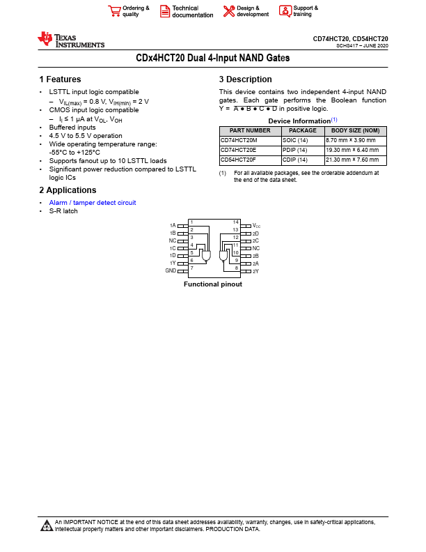
This device contains two independent 4-input NAND gates. Each gate performs the Boolean function Y = A
- B
- C
- D in positive logic.
Device Information(1)
PART NUMBER
PACKAGE
BODY SIZE (NOM)
CD74HCT20M
SOIC (14)
8.70 mm × 3.90 mm
CD74HCT20E
PDIP...