CD74HC04E Overview
Key Specifications
Package: PDIP
Mount Type: Through Hole
Pins: 14
Max Voltage (typical range): 6 V
Description
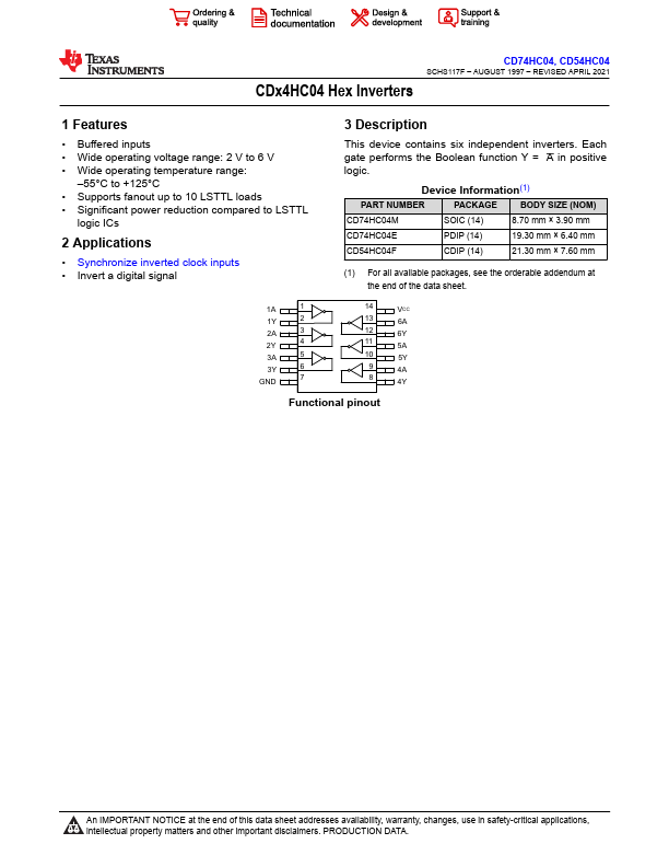
This device contains six independent inverters. Each gate performs the Boolean function Y = A in positive logic.
Key Features
- Buffered inputs
- Wide operating voltage range: 2 V to 6 V
- Wide operating temperature range: –55°C to +125°C
- Supports fanout up to 10 LSTTL loads
- Significant power reduction compared to LSTTL logic ICs