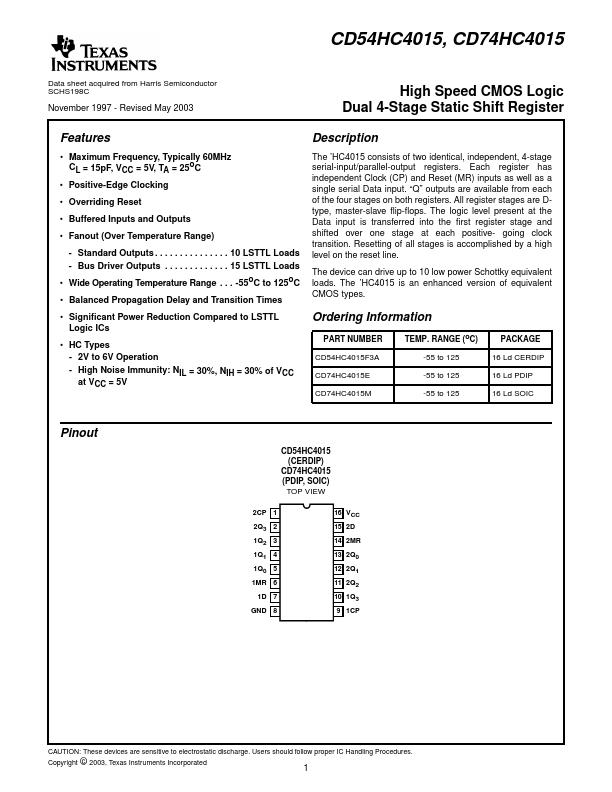
CD74HC4015
Description
Maximum Frequency, Typically 60MHz CL = 15pF, VCC = 5V, TA = 25oC Positive-Edge Clocking Overriding Reset Buffered Inputs and Outputs Fanout (Over Temperature Range) Wide Operating Temperature Range . . . -55oC to 125oC Balanced Propagation Delay and Transition Times Significant Power Reduction Compared to LSTTL Logic ICs HC Types - 2V to 6V Operation - High Noise Immunity: NIL = 30%, NIH = 30% of VCC at VCC = 5V The ’HC4015 consists of two identical, independent, 4-stage serial-input/parallel-output registers. Each register has independent Clock (CP) and Reset (MR) inputs as well as a single serial Data input. “Q” outputs are available from each of the four stages on both registers.