Datasheet4U Logo Datasheet4U.com

CD74HC4511 - BCD-TO-7 SEGMENT LATCH/DECODER/DRIVERS

Download the CD74HC4511 datasheet PDF. This datasheet also covers the CD74HCT4511 variant, as both devices belong to the same bcd-to-7 segment latch/decoder/drivers family and are provided as variant models within a single manufacturer datasheet.

General Description

The CD54HC4511, CD74HC4511, and CD74HCT4511 are BCD-to-7 segment latch/decoder/ drivers with four address inputs (D0

latches to store the BCD inputs.

Key Features

  • 2-V to 6-V VCC operation ('HC4511).
  • 4.5-V to 5.5-V VCC operation (CD74HCT4511).
  • High-output sourcing capability.
  • 7.5 mA at 4.5 V (CD74HCT4511).
  • 10 mA at 6 V ('HC4511).
  • Input latches for BCD code storage.
  • Lamp test and blanking capability.
  • Balanced propagation delays and transition times.
  • Significant power reduction compared to LSTTL logic IC's.
  • 'HC4511.
  • High noise immunity, NIL or NIH = 30% of VCC.

📥 Download Datasheet

Note: The manufacturer provides a single datasheet file (CD74HCT4511-etcTI.pdf) that lists specifications for multiple related part numbers.

Full PDF Text Transcription (Reference)

The following content is an automatically extracted verbatim text from the original manufacturer datasheet and is provided for reference purposes only.

View original datasheet text
CD54HC4511, CD74HC4511, CD74HCT4511 SCHS279E – DECEMBER 1998 – REVISED AUGUST 2022 
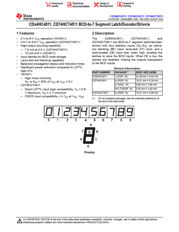
CDx4HC4511, CD74HCT4511 BCD-to-7 Segment Latch/Decoder/Drivers 1 Features • 2-V to 6-V VCC operation ('HC4511) • 4.5-V to 5.5-V VCC operation (CD74HCT4511) • High-output sourcing capability – 7.5 mA at 4.5 V (CD74HCT4511) – 10 mA at 6 V ('HC4511) • Input latches for BCD code storage • Lamp test and blanking capability • Balanced propagation delays and transition times • Significant power reduction compared to LSTTL logic IC's • 'HC4511 – High noise immunity, NIL or NIH = 30% of VCC at VCC = 5 V • CD74HCT4511 – Direct LSTTL input logic compatibility, VIL = 0.