CD74HCT365
Overview
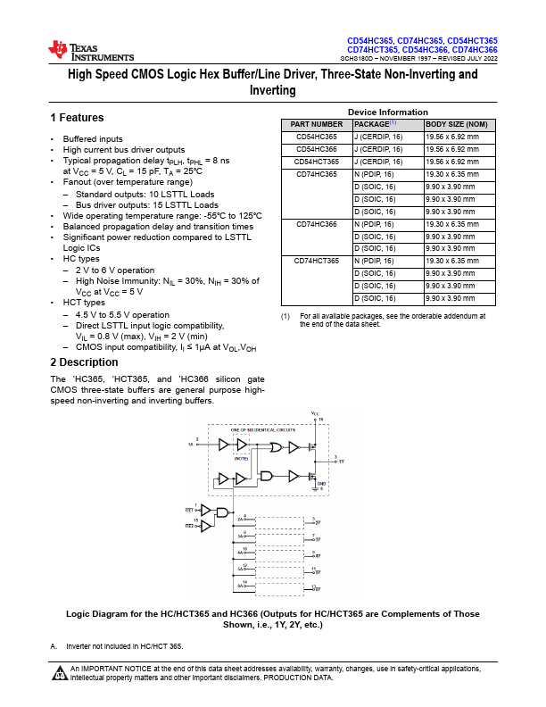
The ’HC365, ’HCT365, and ’HC366 silicon gate CMOS three-state buffers are general purpose highspeed non-inverting and inverting buffers. Device Information PART NUMBER PACKAGE(1) BODY SIZE (NOM) CD54HC365 J (CERDIP, 16) 19.56 x 6.92 mm CD54HC366 J (CERDIP, 16) 19.56 x 6.92 mm CD54HCT365 J (CERDIP, 16) 19.56 x 6.92 mm CD74HC365 N (PDIP, 16) 19.30 x 6.35 mm D (SOIC, 16) 9.90 x 3.90 mm D (SOIC, 16) 9.90 x 3.90 mm D (SOIC, 16) 9.90 x 3.90 mm CD74HC366 N (PDIP, 16) 19.30 x 6.35 mm D (SOIC, 16) 9.90 x 3.90 mm D (SOIC, 16) 9.90 x 3.90 mm CD74HCT365 N (PDIP, 16) 19.30 x 6.35 mm D (SOIC, 16) 9.90 x 3.90 mm D (SOIC, 16) 9.90 x 3.90 mm D (SOIC, 16) 9.90 x 3.90 mm (1) For all available packages, see the orderable addendum at the end of the data sheet.
- Buffered inputs
- High current bus driver outputs
- Typical propagation delay tPLH, tPHL = 8 ns at VCC = 5 V, CL = 15 pF, TA = 25℃
- Fanout (over temperature range) - Standard outputs: 10 LSTTL Loads - Bus driver outputs: 15 LSTTL Loads
- Wide operating temperature range: -55℃ to 125℃
- Balanced propagation delay and transition times
- Significant power reduction compared to LSTTL Logic ICs
- HC types - 2 V to 6 V operation - High Noise Immunity: NIL = 30%, NIH = 30% of VCC at VCC = 5 V
- HCT types - 4.5 V to 5.5 V operation - Direct LSTTL input logic compatibility, VIL = 0.8 V (max), VIH = 2 V (min) - CMOS input compatibility, II ≤ 1µA at VOL,VOH