Datasheet4U Logo Datasheet4U.com

CDCLVC1106 - 3.3-V and 2.5-V LVCMOS High-Performance Clock Buffer

Download the CDCLVC1106 datasheet PDF. This datasheet also covers the CDCLVC1102 variant, as both devices belong to the same 3.3-v and 2.5-v lvcmos high-performance clock buffer family and are provided as variant models within a single manufacturer datasheet.

General Description

The CDCLVC11xx is a modular, high-performance, low-skew, general-purpose clock buffer family from Texas Instruments.

The entire family is designed with a modular approach in mind.

It is intended to round up TI's series of LVCMOS clock generators.

Key Features

  • 1 High-Performance 1:2, 1:3, 1:4, 1:6, 1:8, 1:10, 1:12 LVCMOS Clock Buffer Family.
  • Very Low Pin-to-Pin Skew < 50 ps.
  • Very Low Additive Jitter < 100 fs.
  • Supply Voltage: 3.3 V or 2.5 V.
  • fmax = 250 MHz for 3.3 V fmax = 180 MHz for 2.5 V.
  • Operating Temperature Range:.
  • 40°C to 85°C.
  • Available in 8-, 14-, 16-, 20-, 24-Pin TSSOP Package (All Pin-Compatible) 2.

📥 Download Datasheet

Note: The manufacturer provides a single datasheet file (CDCLVC1102-etcTI.pdf) that lists specifications for multiple related part numbers.

Full PDF Text Transcription (Reference)

The following content is an automatically extracted verbatim text from the original manufacturer datasheet and is provided for reference purposes only.

View original datasheet text
Product Folder Order Now Technical Documents Tools & Software Support & Community CDCLVC1102, CDCLVC1103, CDCLVC1104 CDCLVC1106, CDCLVC1108, CDCLVC1110, CDCLVC1112 SCAS895B – MAY 2010 – REVISED FEBRUARY 2017 
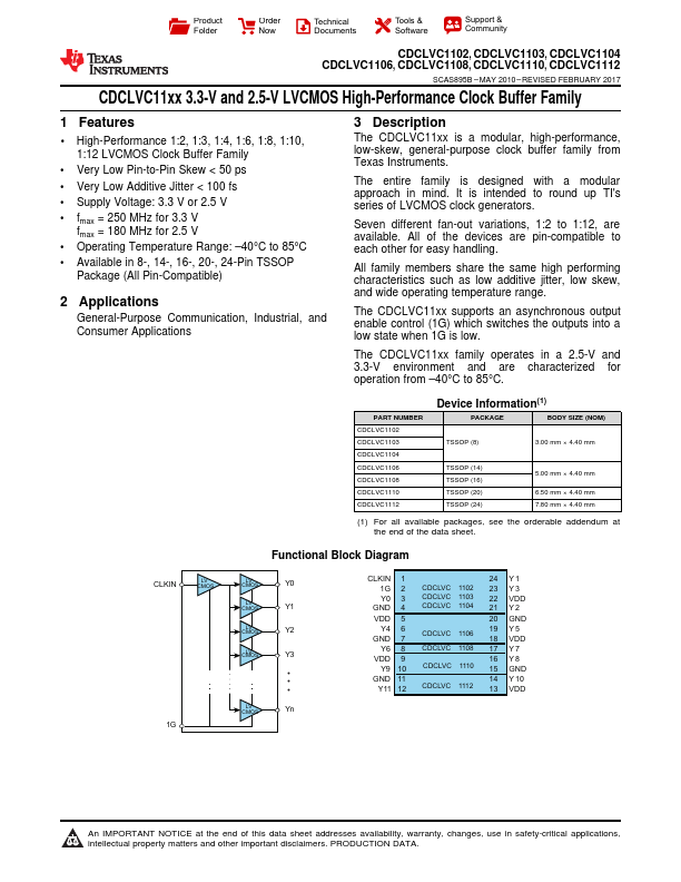
CDCLVC11xx 3.3-V and 2.5-V LVCMOS High-Performance Clock Buffer Family 1 Features •1 High-Performance 1:2, 1:3, 1:4, 1:6, 1:8, 1:10, 1:12 LVCMOS Clock Buffer Family • Very Low Pin-to-Pin Skew < 50 ps • Very Low Additive Jitter < 100 fs • Supply Voltage: 3.3 V or 2.5 V • fmax = 250 MHz for 3.3 V fmax = 180 MHz for 2.