CDCLVP110
Description
The CDCLVP110 clock driver distributes one differential clock pair of either LVPECL or HSTL (selectable) input, (CLK0, CLK1) to ten pairs of differential LVPECL clock (Q0, Q9) outputs with minimum skew for clock distribution. The CDCLVP110 can accept two clock sources into an input multiplexer.
Key Features
- Distributes One Differential Clock Input Pair LVPECL/HSTL to 10 Differential LVPECL Clock Outputs
- Fully compatible With LVECL/LVPECL/HSTL
- Single Supply Voltage Required, ±3.3-V or ±2.5-V Supply
- Selectable Clock Input Through CLK_SEL
- Low-Output Skew (Typ 15 ps) for Clock-Distribution Applications
- VBB Reference Voltage Output for Single-Ended Clocking
- Available in a 32-Pin LQFP Package
- Frequency Range From DC to 3.5 GHz
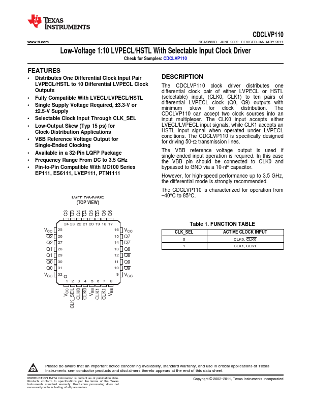
- Pin-to-Pin compatible With MC100 Series EP111, ES6111, LVEP111, PTN1111 spacer spacer LQFP PACKAGE (TOP VIEW)