CDCM1804
Description
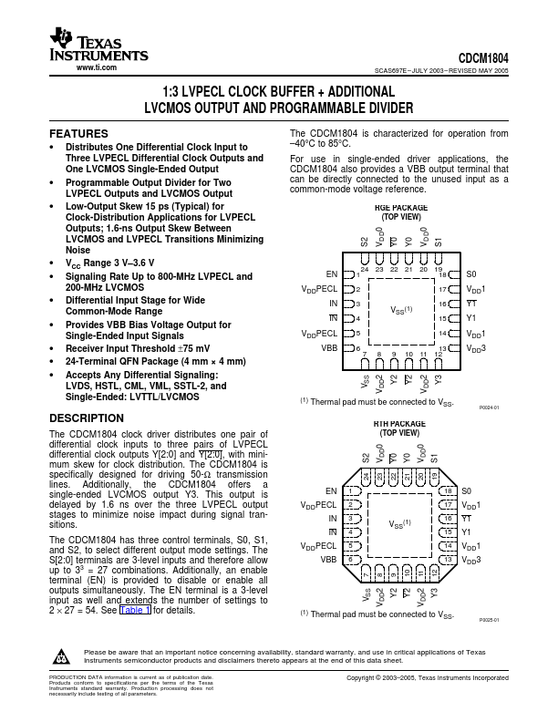
The CDCM1804 clock driver distributes one pair of differential clock inputs to three pairs of LVPECL differential clock outputs Y[2:0] and Y[2:0], with minimum skew for clock distribution.
Key Features
- Distributes One Differential Clock Input to Three LVPECL Differential Clock Outputs and One LVCMOS Single-Ended Output
- Programmable Output Divider for Two LVPECL Outputs and LVCMOS Output
- VCC Range 3 V–3.6 V
- Signaling Rate Up to 800-MHz LVPECL and
- Provides VBB Bias Voltage Output for Single-Ended Input Signals
- Receiver Input Threshold ±75 mV
- 24-Terminal QFN Package (4 mm × 4 mm)
- Accepts Any Differential Signaling: LVDS, HSTL, CML, VML, SSTL-2, and Single-Ended: LVTTL/LVCMOS