CDCVF25081 Overview
Key Specifications
Package: SOIC
Mount Type: Surface Mount
Pins: 16
Operating Voltage: 3.3 V
Description
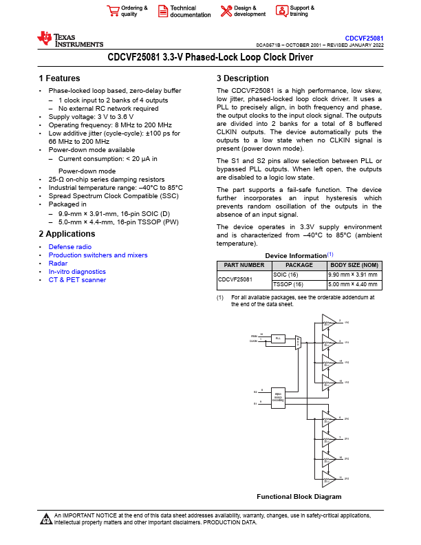
The CDCVF25081 is a high performance, low skew, low jitter, phased-locked loop clock driver. It uses a PLL to precisely align, in both frequency and phase, the output clocks to the input clock signal.
Key Features
- Phase-locked loop based, zero-delay buffer – 1 clock input to 2 banks of 4 outputs – No external RC network required
- Supply voltage: 3 V to 3.6 V
- Operating frequency: 8 MHz to 200 MHz
- Low additive jitter (cycle-cycle): ±100 ps for 66 MHz to 200 MHz
- Power-down mode available – Current consumption: < 20 µA in Power-down mode