CSD16406Q3
CSD16406Q3 is N-Channel Power MOSFET manufactured by Texas Instruments.
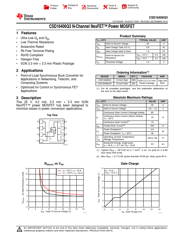
Features
- 1 Ultra-Low Qg and Qgd
- Low Thermal Resistance
- Avalanche Rated
- Pb Free Terminal Plating
- Ro HS pliant
- Halogen Free
- SON 3.3 mm × 3.3 mm Plastic Package
2 Applications
- Point-of-Load Synchronous Buck Converter for Applications in Networking, Tele, and puting Systems
- Optimized for Control or Synchronous FET Applications
Product Summary
TA = 25°C
Drain-to-Source Voltage
Qg
Gate Charge Total (4.5 V)
Qgd
Gate Charge Gate to Drain
RDS(on)
Drain-to-Source On Resistance
Vth
Threshold Voltage
TYPICAL VALUE
VGS = 4.5 V
VGS = 10 V
UNIT V n C n C mΩ mΩ V
DEVICE CSD16406Q3 CSD16406Q3T
. Ordering Information(1)
MEDIA
PACKAGE
SHIP
13-Inch Reel 2500 SON 3.3 x 3.3 mm Tape...