Datasheet4U Logo Datasheet4U.com

CSD18501Q5A - Power MOSFETs

General Description

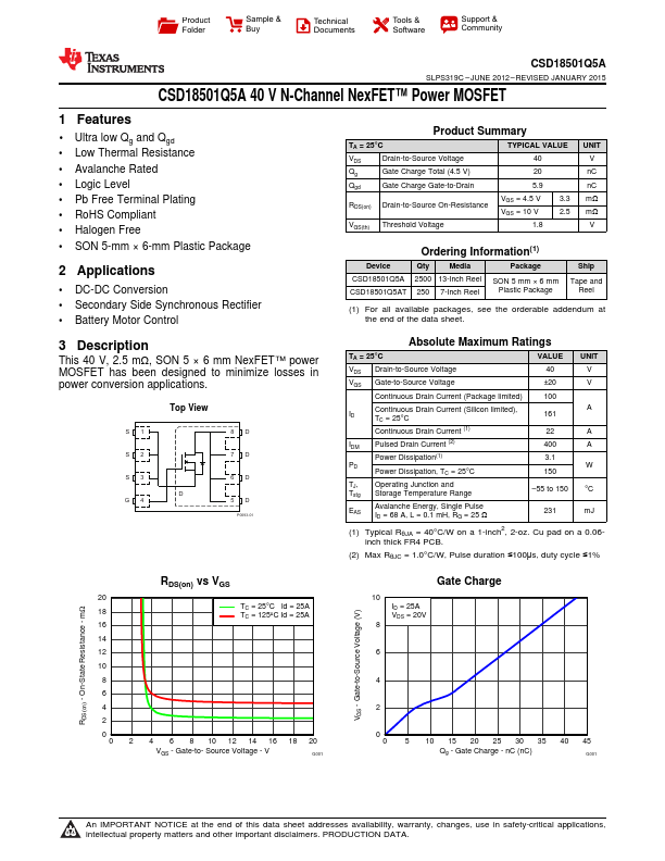
This 40 V, 2.5 mΩ, SON 5 × 6 mm NexFET™ power MOSFET has been designed to minimize losses in power conversion applications.

Key Features

  • 1 Ultra low Qg and Qgd.
  • Low Thermal Resistance.
  • Avalanche Rated.
  • Logic Level.
  • Pb Free Terminal Plating.
  • RoHS Compliant.
  • Halogen Free.
  • SON 5-mm × 6-mm Plastic Package 2.

📥 Download Datasheet

Full PDF Text Transcription (Reference)

The following content is an automatically extracted verbatim text from the original manufacturer datasheet and is provided for reference purposes only.

View original datasheet text
Product Folder Sample & Buy Technical Documents Tools & Software Support & Community CSD18501Q5A SLPS319C – JUNE 2012 – REVISED JANUARY 2015 CSD18501Q5A 40 V N-Channel NexFET™ Power MOSFET 1 Features •1 Ultra low Qg and Qgd • Low Thermal Resistance • Avalanche Rated • Logic Level • Pb Free Terminal Plating • RoHS Compliant • Halogen Free • SON 5-mm × 6-mm Plastic Package 2 Applications • DC-DC Conversion • Secondary Side Synchronous Rectifier • Battery Motor Control Product Summary TA = 25°C VDS Drain-to-Source Voltage Qg Gate Charge Total (4.5 V) Qgd Gate Charge Gate-to-Drain RDS(on) Drain-to-Source On-Resistance VGS(th) Threshold Voltage TYPICAL VALUE 40 20 5.9 VGS = 4.5 V 3.3 VGS = 10 V 2.5 1.