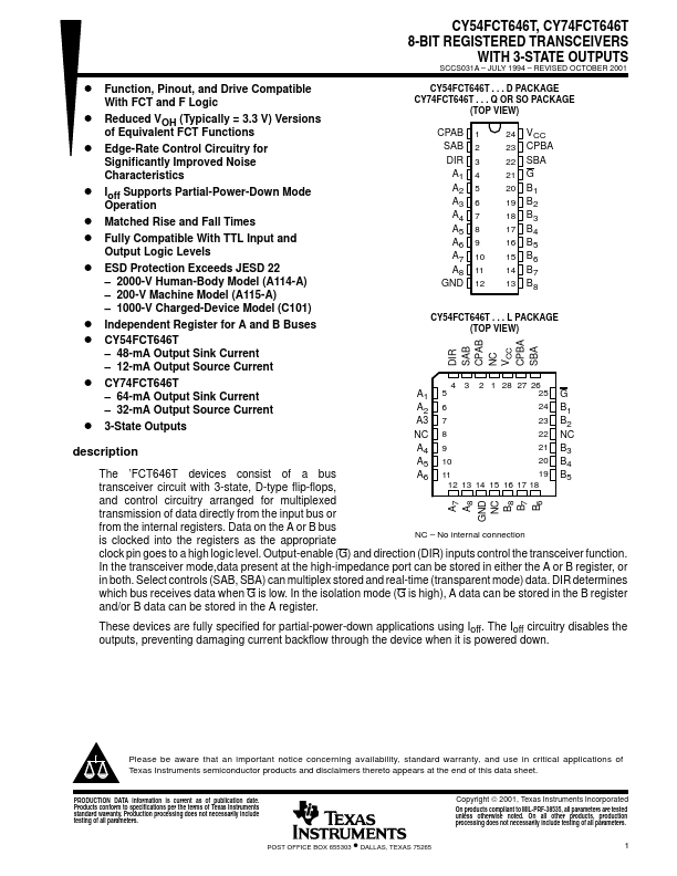
CY74FCT646T Description
Data on the A or B bus is clocked into the registers as the appropriate NC No internal connection clock pin goes to a high logic level. Output-enable (G) and direction (DIR) inputs control the transceiver function. In the transceiver mode,data present at the high-impedance port can be stored in either the A or B register, or in both.