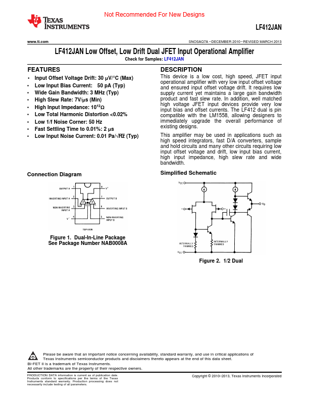
LF412JAN Overview
Description
This device is a low cost, high speed, JFET input operational amplifier with very low input offset voltage and ensured input offset voltage drift. It requires low supply current yet maintains a large gain bandwidth product and fast slew rate.
Key Features
- 23 Input Offset Voltage Drift: 30 μV/°C (Max)
- Low Input Bias Current: 50 pA (Typ)
- Wide Gain Bandwidth: 3 MHz (Typ)
- High Slew Rate: 7V/μs (Min)
- High Input Impedance: 1012Ω
- Low Total Harmonic Distortion <0.02%
- Low 1/f Noise Corner: 50 Hz
- Fast Settling Time to 0.01%: 2 μs
- Low Input Noise Current: 0.01 Pa/√Hz (Typ)