LMH6504
LMH6504 is Variable Gain Amplifier manufactured by Texas Instruments.
URES
- 23 VS = ±5V, TA = 25°C, RF = 1 KΩ, RG = 100Ω, RL = 100Ω, AV = AVMAX = 9.7V/V, Typical values unless specified.
- - 3 d B BW 150 MHz
- Gain control BW 150 MHz
- Adjustment range (<10 MHz) 80 d B
- Output offset voltage ±55 m V
- Gain matching (limit) ±0.42 d B
- Supply voltage range 7V to 12V
- Slew rate (inverting) 1500 V/μs
- Supply Current (no load) 11 m A
- Linear Output Current ±60 m A
- Output Voltage Swing ±2.2V
- Input Noise Voltage 4.4 n V/√Hz
- Input Noise Current 2.6 p A/√Hz
- THD (20 MHz, RL = 100Ω, VO = 2 VPP)
- 45 d Bc
- Replacement for CLC5523
APPLICATIONS
- Variable attenuator
- AGC
- Voltage controlled filter
- Video imaging processing
DESCRIPTION
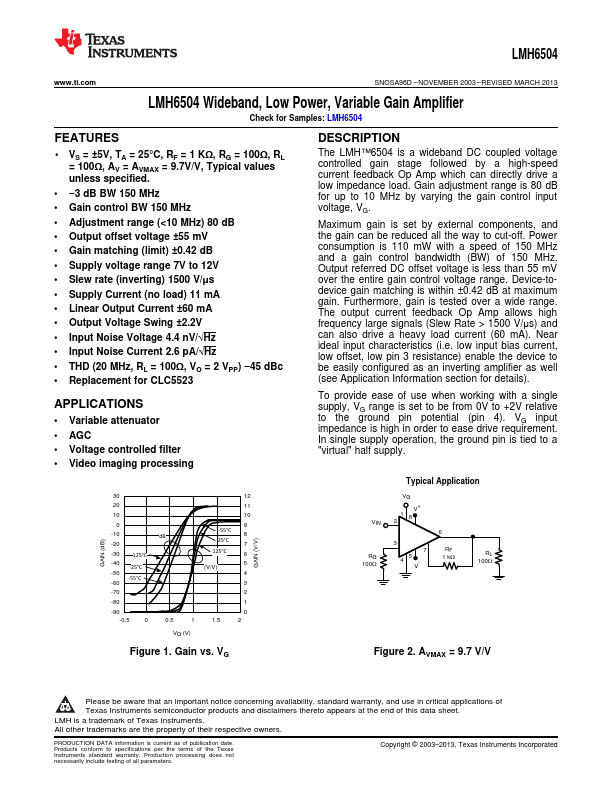
The LMH™6504 is a wideband DC coupled voltage controlled gain stage followed by a high-speed current feedback Op Amp which can directly drive a low impedance load. Gain adjustment range is 80 d B for up to 10 MHz by varying the gain control input voltage, VG.
Maximum gain is set by external ponents, and the gain can be reduced all the way to cut-off. Power consumption is 110 m W with a speed of 150 MHz and a gain control bandwidth (BW) of 150 MHz. Output referred DC offset voltage is less than 55 m V over the entire gain control voltage range. Device-todevice gain matching is within ±0.42 d B at maximum gain. Furthermore, gain is tested over a wide range. The output current feedback Op Amp allows high frequency large signals (Slew Rate > 1500 V/μs) and can also drive a heavy load current (60 m A). Near ideal input characteristics (i.e. low input bias current, low offset, low pin 3 resistance) enable the device to be easily configured as an inverting amplifier as well (see Application Information section for details).
To provide ease of use when working with a single supply, VG range is set to be from 0V to +2V relative to the ground pin potential (pin 4). VG input impedance is high in order to ease drive requirement. In single supply operation, the ground pin is tied to a "virtual" half supply.
GAIN (d B) GAIN...