LMH6626
Features
- 1 VS = ±6 V, TA = 25°C, AV = 20 (Typical Values Unless Specified)
- Gain Bandwidth (LMH6624) 1.5 GHz
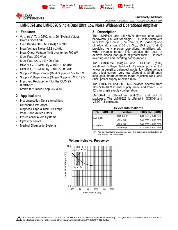
- Input Voltage Noise 0.92 n V/√Hz
- Input Offset Voltage (limit over temp) 700 µV
- Slew Rate 350 V/μs
- Slew Rate (AV = 10) 400 V/μs
- HD2 at f = 10 MHz, RL = 100 Ω
- 63 d Bc
- HD3 at f = 10 MHz, RL = 100 Ω
- 80 d Bc
- Supply Voltage Range (Dual Supply) 2.5 V to 6 V
- Supply Voltage Range (Single Supply) 5 V to 12 V
- Improved Replacement for the CLC425
(LMH6624)
- Stable for Closed Loop |AV| ≥ 10
2 Applications
- Instrumentation Sense Amplifiers
- Ultrasound Pre-amps
- Magnetic Tape & Disk Pre-amps
- Wide Band Active Filters
- Professional Audio Systems
- Opto-electronics
- Medical Diagnostic Systems
3 Description
The LMH6624 and LMH6626 devices offer wide bandwidth (1.5 GHz for single, 1.3 GHz for dual) with very low input noise (0.92 n V/√Hz, 2.3 p A/√Hz) and ultra-low dc errors (100 μV VOS, ±0.1 μV/°C drift) providing very precise operational amplifiers with wide dynamic...