LMK00804B-Q1
Description
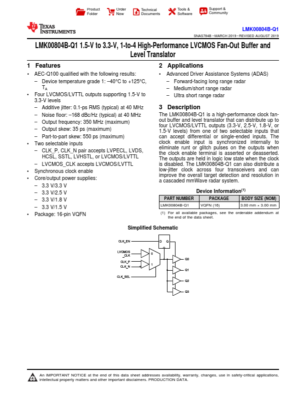
The LMK00804B-Q1 is a high-performance clock fanout buffer and level translator that can distribute up to four LVCMOS/LVTTL outputs (3.3-V, 2.5-V, 1.8-V, or 1.5-V levels) from one of two selectable inputs that can accept differential or single-ended inputs.
Key Features
- 1 AEC-Q100 qualified with the following results: – Device temperature grade 1: –40°C to +125°C, TA
- Two selectable inputs – CLK_P, CLK_N pair accepts LVPECL, LVDS, HCSL, SSTL, LVHSTL, or LVCMOS/LVTTL – LVCMOS_CLK accepts LVCMOS/LVTTL
- Synchronous clock enable
- Core/output power supplies
- Package: 16-pin VQFN
Applications
- Advanced Driver Assistance Systems (ADAS) – Forward-facing long range radar – Medium/short range radar – Ultra short range radar