LMK1C1103
Features
- High-performance 1:2, 1:3 or 1:4 LVCMOS clock buffer
- Very low output skew < 50 ps
- Extremely low additive jitter < 50 fs maximum
- 7.5 fs typical at VDD = 3.3 V
- 10 fs typical at VDD = 2.5 V
- 19.2 fs typical at VDD = 1.8 V
- Very low propagation delay < 3 ns
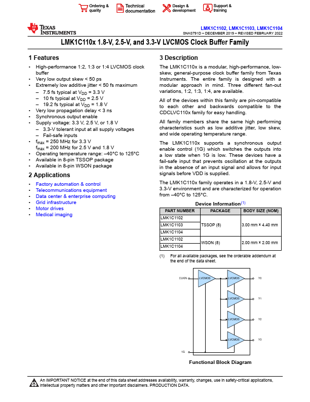
- Synchronous output enable
- Supply voltage: 3.3 V, 2.5 V, or 1.8 V
- 3.3-V tolerant input at all supply voltages
- Fail-safe inputs
- fmax = 250 MHz for 3.3 V fmax = 200 MHz for 2.5 V and 1.8 V
- Operating temperature range:
- 40°C to 125°C
- Available in 8-pin TSSOP package
- Available in 8-pin WSON package
2 Applications
- Factory automation & control
- Telemunications equipment
- Data center & enterprise puting
- Grid infrastructure
- Motor drives
- Medical imaging
3 Description
The LMK1C110x is a modular, high-performance, lowskew, general-purpose clock buffer family from Texas Instruments. The entire family is designed with a modular approach in mind. Three different fan-out variations, 1:2, 1:3, 1:4, are...